
Digital/analogue conversion apparatus

a digital/analog conversion and digital/analog technology, applied in the direction of code conversion, frequency response correction, filters, etc., can solve the problems of non-linear noise, difficult to reproduce high-definition audio signals, and inconvenient operation, so as to reduce out-of-band quantization noise and increase in-band noise

Inactive Publication Date: 2013-06-20
TRIGENCE SEMICONDUCTOR INC
View PDF3 Cites 15 Cited by
  • Summary
  • Abstract
  • Description
  • Claims
  • Application Information

AI Technical Summary

Benefits of technology

This approach effectively reduces out-of-band quantization noise and maintains high signal-to-noise ratio (SNR) even with nonuniformity in drive devices, achieving high-resolution analog signal conversion with compact circuitry.

Problems solved by technology

In these conventional examples, because the serial-parallel converted signals are used as they are unadjusted as signals for driving a plurality of circuits the following problems occur: firstly, the manufacturing nonuniformity among current power sources of weighted drive circuits becomes a cause of non-linear noise, and second, when reproducing a digital signal the quantization noise which is generated during reproducing digital signals is superimposed as a noise component in an audible frequency band.
Therefore, these examples suffer from difficulty in reproducing high definition audio signals.
However, a problem remains because even though a speaker drive circuit is driven without attenuating the quantization noise which is pushed out to a frequency higher than the audible frequency band by a digitally modulation using a sigma delta modulator and over sampling, the quantization noise which shifts to a higher frequency band is emitted from the speaker.
The need for a high speed operation in a selection circuit is an serious weakness in the miss match shaping method which uses the DEM method.
Furthermore, this weakness has already been pointed out in U.S. Pat. No. 5,872,532 and is widely known.
In addition, when the order of the delta sigma modulator is increased the operation of the delta sigma modulator becomes unstable.
However, when a pass-band is narrow the decay time constant becomes larger and it becomes impossible to ignore the space occupied by the LPF mounted in a semiconductor integrated device.
In this case, because a large capacitor is often required to reduce a cutoff frequency in addition to an OP amp in order to realize the Switched Capacitor Filter, this method suffers from a significant increase in chip area and consumption of power.

Method used


Image

  • Digital/analogue conversion apparatus
  • Digital/analogue conversion apparatus
  • Digital/analogue conversion apparatus

Examples


example one

[0081]FIG. 6 shows a first example in which an analog FIR filter and a post filter is placed after a cascade type delta sigma modulator of the digital analog conversion apparatus of a preferred embodiment. In the present example, the first stage of the cascade type delta sigma modulator is comprised of a single bit internal modulator and the second stage is comprised of an n bit internal modulator.

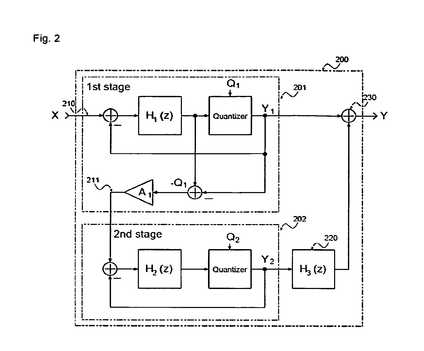
[0082]Here, a digital input signal (510) is input to a first stage internal modulator (201) of the cascade type delta sigma modulator, the second stage internal modulator (202) is connected by a cascade connection to the first stage internal modulator (201), and an output signal (520) output from the first stage internal modulator (201) is input to an analog FIR filter (301). A (1−z−n) calculation of an output signal (530) output from the second stage internal modulator (202) is performed by a digital signal process block (601). An output (631) form the digital signal process block (601) i...

example two

[0090]FIG. 9 shows a second example of the digital analog conversion apparatus of a preferred embodiment. In the present example, the first stage of the cascade type delta sigma modulator is comprised of a single bit internal modulator and the second stage is comprised of an n bit internal modulator. As is shown by the expression 9, when the order of the internal modulator is the first order, the transfer function of the second stage is (1−z−n)·1. Because (1−z−n) is digitally processed, it is necessary to analogically calculate 1. Here, the input signal Y2-m (632), which is converted into a thermometer code by the formatter, is firstly input to the selector (910), and a unit group comprises drive buffers (901), which are connected to each of the bits from the outputs of the selector, and resistance elements (902) in which each end is connected to one of the drive buffer and each other end is connected to an output terminal so that a weighted voltage is added as an analog signal. In ...

example three

[0092]FIG. 10 shows a third example of a digital analog conversion apparatus of a preferred embodiment. In the present example, the first stage of the cascade type delta sigma modulator is comprised of a single bit internal modulator and the second stage is comprised of an n bit internal modulator. As is shown by the expression 10, when the order of the internal modulator is the second order, the transfer function of the second stage is (1−z−n)·(1−z−1). Because (1−z−n) is digitally processed, it is necessary to analogically calculate (1−z−1). Here, the input signal Y2-m (632), which is converted into a thermometer code by the formatter, is firstly input to the selector (1010) and secondly input to one of post filter units (603), which corresponds to each bit of the output (1020) of the selector. A post filter unit (603) is comprised of a delay element (711) formed by a DFF which enables one clock delay, a drive buffer (712) which is connected to an input via a switch (715a) which is...


PUM


Abstract

A digital / analog conversion apparatus to convert a digital signal into an analog signal. The digital / analog conversion apparatus can generate a high-quality analog signal, even when elements configuring the digital / analog conversion apparatus have variance, with high resolution and a small circuit size. The data conversion apparatus is provided with a first data converter to reduce the number of bits of an input signal, a second data converter to convert the format of the first output signal, and a third data converter for conversion into a code which corresponds to the history of the output from the second data converter.

Description

CROSS-REFERENCE TO RELATED APPLICATIONS[0001]This application is a U.S. continuation application filed under 37 USC 1.53 claiming priority benefit of U.S. Ser. No. 12 / 285,323 filed in the United States on Oct. 1, 2008, which is based upon and claims the benefit of priority to U.S. continuation application filed under 35 USC 111(a) claiming benefit under 35 USC 120 and 365(c) of PCT application JP2007 / 060072, filed on May 16, 2007, which claims priority to Japanese Application Nos. 2006-140975 and 2006-277476, respectively filed May 21, 2006 and Oct. 11, 2006, the entire contents of the foregoing applications being incorporated herein by reference.BACKGROUND OF THE INVENTION[0002]1. Field of the Invention[0003]Embodiments relate to a digital / analogue conversion apparatus which converts a digital signal into an analog signal and also relates to applications using the same.[0004]2. Description of the Related Art[0005]U.S. Pat. No. 5,862,237 and U.S. Pat. No. 5,909,496 propose conventio...

Claims


Application Information

Patent Timeline
Patent Type & Authority Applications(United States)
IPC IPC(8): H03G3/20
CPCH03H15/00H03M3/344H03G3/20H03M3/504H03M7/3022H03M3/414H03H17/00H03M3/02H04R1/005H04R3/00H04R3/08H04R17/005
Inventor YASUDA, AKIRAOKAMURA, JUNICHI
Owner TRIGENCE SEMICONDUCTOR INC
Learn More