Light-Emitting Element, Light-Emitting Device, and Electronic Appliance

Active Publication Date: 2009-04-02
SEMICON ENERGY LAB CO LTD
View PDF20 Cites 39 Cited by
  • Summary
  • Abstract
  • Description
  • Claims
  • Application Information

AI Technical Summary

Benefits of technology

[0024]According to the present invention, the rate of transport of holes that are carriers of a light-emitting element can be reduced; therefore, the probability of recombination in the light-emitting layer can be increased, and the emission efficiency of the light-emitting layer can be improved. Furthermore, by combining a structure capable of reducing the rate o

Problems solved by technology

However, as disclosed in Non-patent Document 1, there are problems in that the hole-blocking la

Method used


Image

  • Light-Emitting Element, Light-Emitting Device, and Electronic Appliance
  • Light-Emitting Element, Light-Emitting Device, and Electronic Appliance
  • Light-Emitting Element, Light-Emitting Device, and Electronic Appliance

Examples


embodiment mode 1

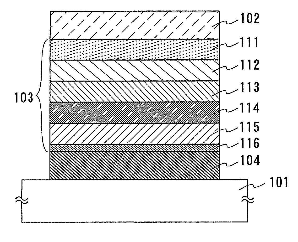
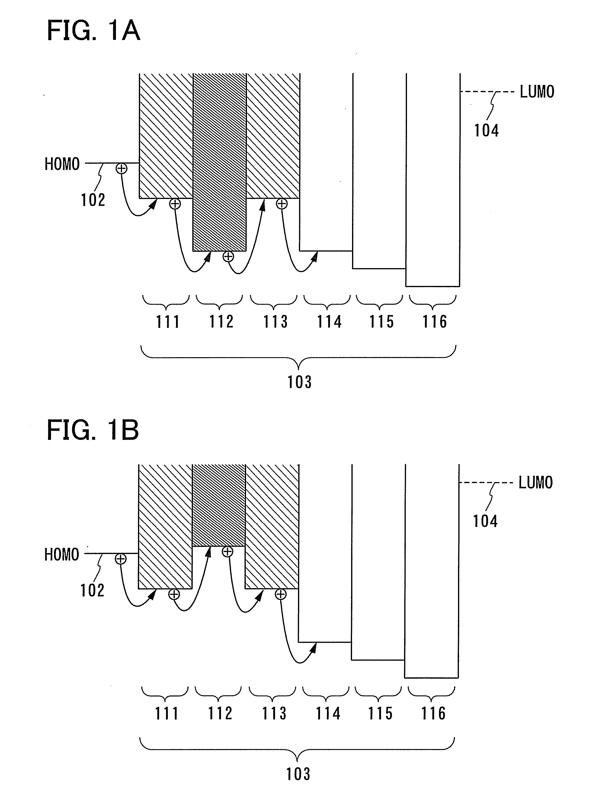
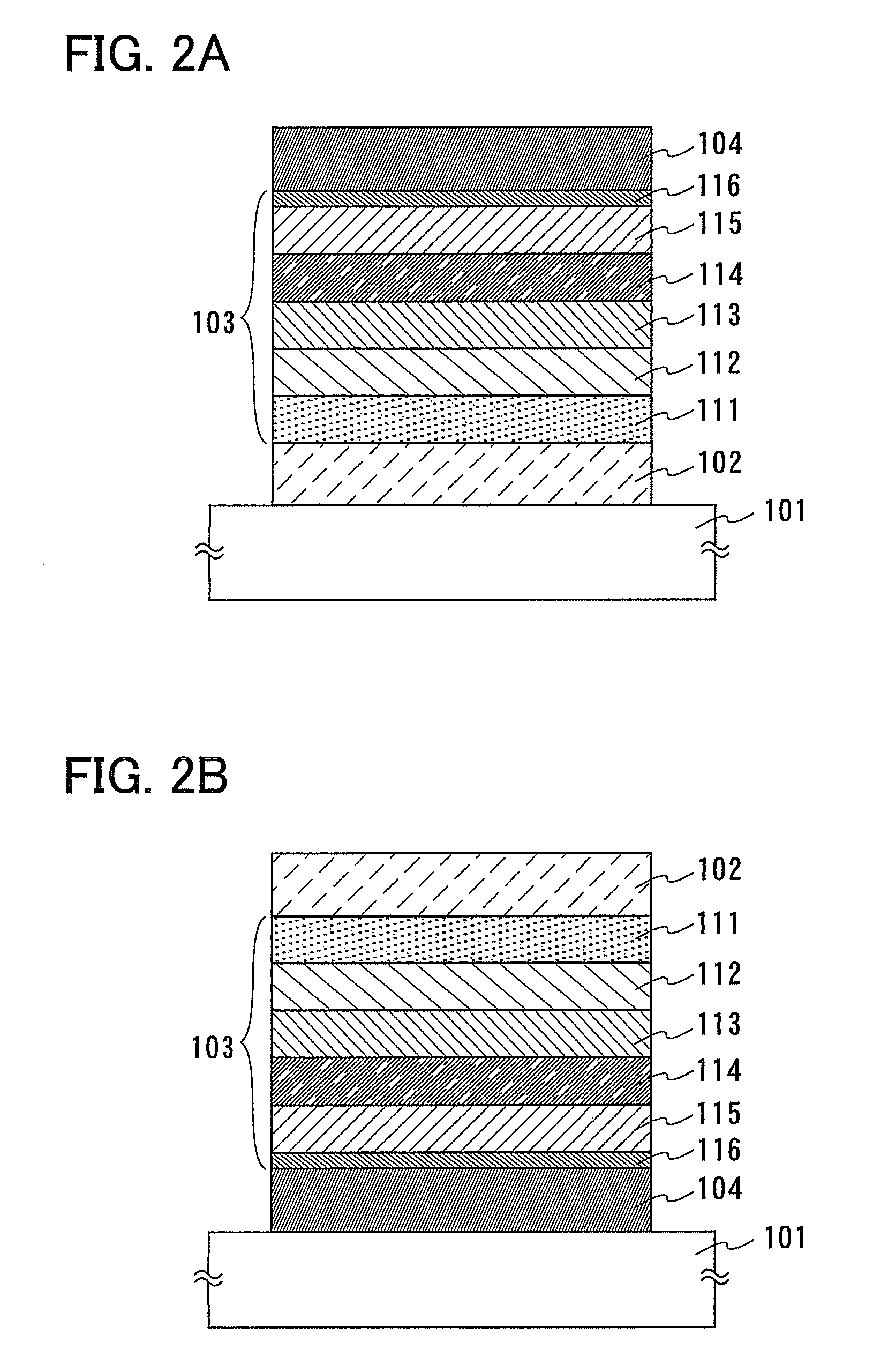
[0064]In Embodiment Mode 1, a light-emitting element of the present invention, which has a structure that reduces the rate of transport of holes that are carriers of the light-emitting element, is described.

[0065]The light-emitting element in Embodiment Mode 1 includes a first electrode functioning as an anode, a second electrode functioning as a cathode, and an EL layer provided between the first electrode and the second electrode. The EL layer may be provided so that it includes at least a hole-injecting layer, a first hole-transporting layer, a second hole-transporting layer, and a light-emitting layer which are stacked in that order from the first electrode side, and that the highest occupied molecular orbital level (HOMO level) of the first hole-transporting layer is deeper (the absolute value is larger) or shallower (the absolute value is smaller) than the HOMO levels of the hole-injecting layer and the second hole-transporting layer. There is no particular limitation on other...

embodiment mode 2

[0127]In Embodiment Mode 2, a light-emitting element of the present invention, which has a structure that reduces the rate of transport of electrons in addition to the structure described in Embodiment Mode 1, which reduces the rate of transport of holes, is described.

[0128]The light-emitting element in Embodiment Mode 2 includes a first electrode, a second electrode, and an EL layer provided between the first electrode and the second electrode. The EL layer may be provided so that it includes at least a hole-injecting layer, a first hole-transporting layer, a second hole-transporting layer, a light-emitting layer, and a carrier control layer which are stacked in that order from the first electrode side, and that the highest occupied molecular orbital level (HOMO level) of the first hole-transporting layer is deeper (the absolute value is larger) or shallower (the absolute value is smaller) than the HOMO levels of the hole-injecting layer and the second hole-transporting layer. Ther...

embodiment mode 3

[0190]In Embodiment Mode 3, a light-emitting element having a plurality of EL layers of the light-emitting elements described in Embodiment Mode 1 and 2 (hereinafter, referred to as a stacked-type element) is described using FIG. 8. This light-emitting element is a stacked-type light-emitting element that has a plurality of EL layers (a first EL layer 803 and a second EL layer 804) between a first electrode 801 and a second electrode 802. Note that although a structure of two EL layers is described in Embodiment Mode 3, a structure of three or more EL layers may be employed.

[0191]In Embodiment Mode 3, the first electrode 801 functions as an anode and the second electrode 802 functions as a cathode. Note that the first electrode 801 and the second electrode 802 can be made to have structures similar to those described in Embodiment Mode 1. Further, for the plurality of EL layers (the first EL layer 803 and the second EL layer 804), structures similar to those described in Embodiment ...


PUM


Abstract

In a light-emitting element including an EL layer between a pair of electrodes, between an electrode functioning as an anode and a fourth layer having a light-emitting property (light-emitting layer), the EL layer includes at least a first layer having a hole-injecting property (hole-injecting layer), a second layer having a hole-transporting property (first hole-transporting layer), and a third layer having a hole-transporting property (second hole-transporting layer). The absolute value of the highest occupied molecular orbital level (HOMO level) of the second layer is larger than the absolute value of the highest occupied molecular orbital level (HOMO level) of each of the first layer and the third layer. With such a structure, the rate of transport of holes injected from the electrode functioning as an anode is reduced and emission efficiency of the light-emitting element is improved.

Description

BACKGROUND OF THE INVENTION[0001]1. Field of the Invention[0002]The present invention relates to a current excitation type light-emitting element in which a light-emitting substance is interposed between a pair of electrodes, and a light-emitting device and an electronic appliance each having such a light-emitting element.[0003]2. Description of the Related Art[0004]In recent years, research and development have been actively conducted on light-emitting elements using electroluminescence. In a basic structure of such a light-emitting element, a layer containing a substance having a light-emitting property is interposed between a pair of electrodes. By applying voltage to this element, light emission from the substance having a light-emitting property can be obtained.[0005]Such a light-emitting element, which is a self-luminous element, is advantageous in that pixel visibility is high compared to that of a liquid crystal display, that no backlight is needed, and the like and thought ...

Claims


Application Information

Patent Timeline
IPC IPC(8): H01J1/62
CPCH01L2251/552H01L51/5048H10K50/14H10K2101/30H05B33/14H05B33/22
Inventor SHITAGAKI, SATOKOSUZUKI, TSUNENORISEO, SATOSHI
Owner SEMICON ENERGY LAB CO LTD
Why Eureka
Try Eureka