Flash memory

a flash memory and flash technology, applied in the field of flash memory, can solve the problems of loss of all electric charges, embedded flash memory occupies an even larger area, and flash memory cannot allow random access to data for reading, so as to reduce the manufacturing of flash memory, improve the retention of stored data, and facilitate the integration into the cmos process

Inactive Publication Date: 2009-04-02
EON SILICON SOLUTION
View PDF15 Cites 20 Cited by
  • Summary
  • Abstract
  • Description
  • Claims
  • Application Information

AI Technical Summary

Benefits of technology

[0011]A further object of the present invention is to provide a flash memory applied in NAND and/or NOR flash memory. The flash memory of the present invention has an SONOS cell structure, and uses an ONO film to replace a floating gate to enable miniaturization of the flash memory without the problem of data mutual interference, so that the retention of stored data is largely improved.
[0012]A still further object of the present invention is to provide a flash memory applied in NAND and/or NOR flash memory. The flash memory of the present invention has an SONOS cell structure and uses an ONO film to replace a floating gate, enabling it to be easily integrated into a CMOS process to largely reduce the manufacturing thereof, and is therefore very suitable for use as a memory element.
[0013]To achieve the above and other objects, the flash memory of the present invention has an SONOS cell structure, uses channel-hot-electron injection as a write mechanism thereof to have a localized trapping characteristic, and uses hot-hole injection as an erase mechanism thereof. And, the flash memory of the present invention uses an ONO film to replace a floating gate to solve the problem of an entire leakage caused by a local leakage of the floating gate. The flash memory of the present invention may be miniaturized without the problem of data mutual interference, so that the retention of stored data is largely improved. Moreover, the flash memory of the present invention can be easily integrated into a CMOS process to largely reduce the manufacturing thereof, and is therefore very suitable for use as a memory element.
[0014]The flash memory with the SONOS structure according to the present invention uses the channel-hot-electron injection and the hot-hole injection as a write mechanism and an erase mechanism thereof, respectively. The use of the channel-hot-electron injection as the write mechanism gives the flash memory of the present invention the characteristic of localized trapping, which is very helpful in multi-bit memory. The flash memory of the pre

Problems solved by technology

However, the NAND flash memory does not allow random access of data for reading, and must output data sequentially.
This would result in an embedded flash memory occupying an even larger area.
Moreover, a main problem with the flash memory with floating gate poly1 is that, any small defect in the oxide insulating layers surroundi

Method used


Image

  • Flash memory
  • Flash memory
  • Flash memory

Examples


Embodiment Construction

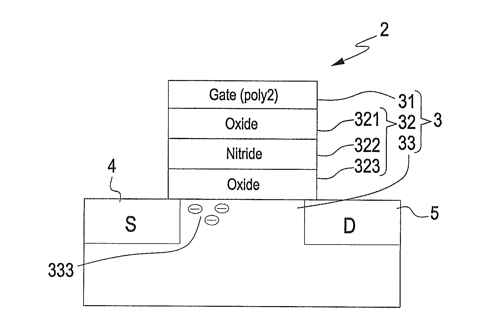
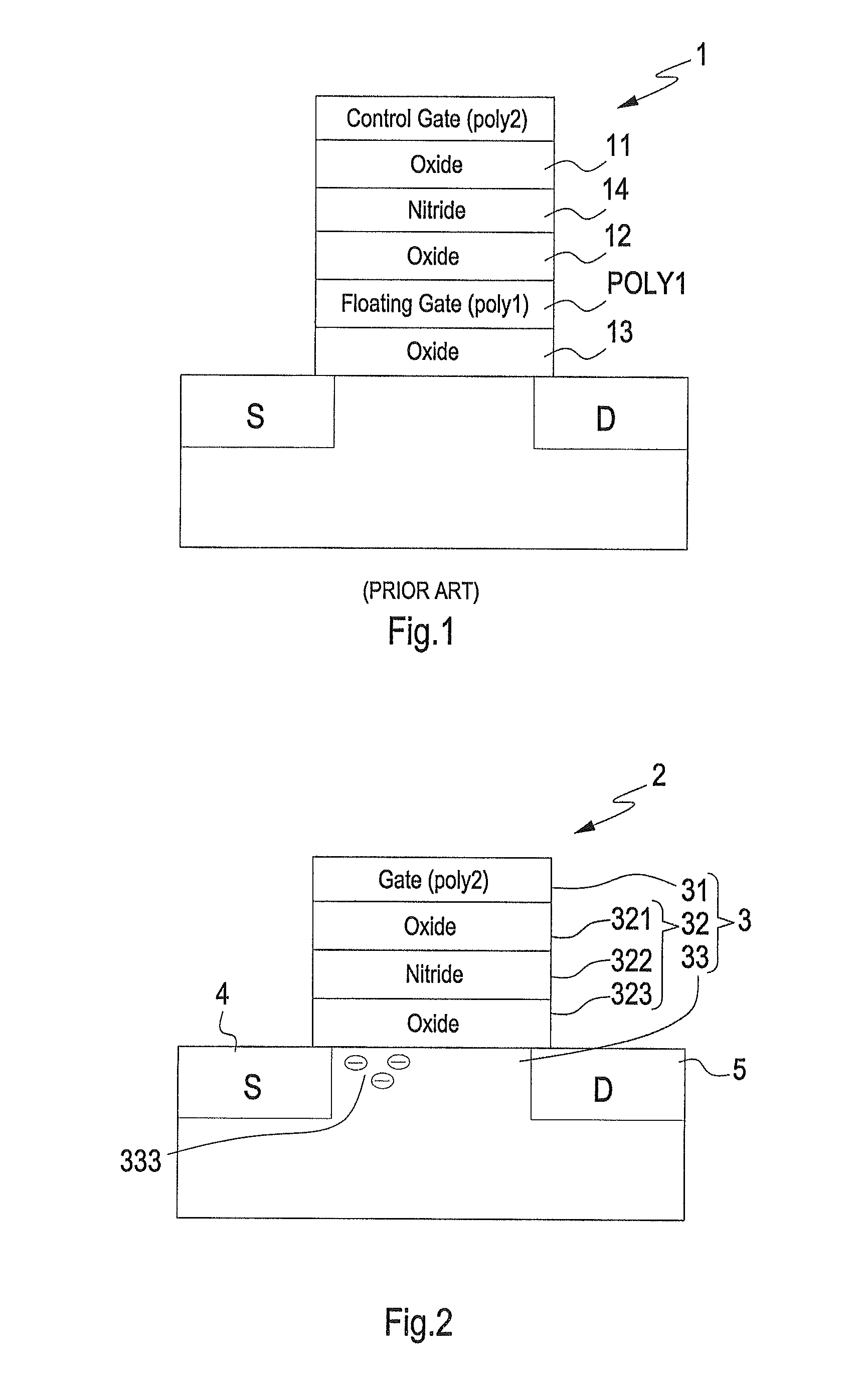
[0029]Please refer to FIG. 2 that is a conceptual view showing the structure of a flash memory according to an embodiment of the present invention. In the embodiment illustrated in FIG. 2, the flash memory is an n-channel silicon-oxide-nitride-oxide-silicon (SONOS) flash memory 2 consisting of a SONOS structure 3, a source 4, a drain 5, and a silicon substrate. The source 4 and the drain 5 may be exchanged in their position. That is, when the source 4 is located at the left side of the flash memory 2, the drain 5 is at the right side of the flash memory 2; and, when the source 4 is located at the right side of the flash memory 2, the drain 5 is at the left side of the flash memory 2.

[0030]The SONOS structure 3 includes a gate 31, an oxide-nitride-oxide (ONO) structure 32, and a silicon channel 33. The ONO structure 32 includes an upper oxide layer 321, a nitride layer 322, and a lower oxide layer 323. In the illustrated embodiment, the upper oxide layer 321 is of a capping oxide lay...


PUM


Abstract

A flash memory applied in NAND and/or NOR flash memory has a silicon-oxide-nitride-oxide-silicon cell structure, uses channel-hot-electron injection as a write mechanism thereof to have a localized trapping characteristic, and uses hot-hole injection as an erase mechanism thereof. The flash memory uses an oxide-nitride-oxide structure to replace a floating gate, and thereby solves the problem of an entire leakage caused by a local leakage of the floating gate. The flash memory may be miniaturized without the problem of data mutual interference, and may be easily integrated into the CMOS process to largely reduce the manufacturing cost thereof. Meanwhile, the flash memory also enables faster program time and erase time.

Description

FIELD OF THE INVENTION[0001]The present invention relates to a flash memory, and more particularly, to a flash memory having a silicon-oxide-nitride-oxide-silicon cell structure. The flash memory uses channel-hot-electron injection as a write mechanism thereof to have the localized trapping characteristic, and uses hot hole injection as an erase mechanism thereof to provide better program, read, and erase efficiency, faster program, read, and erase time, and larger program, read, and erase window than other types of flash memory. Moreover, the flash memory of the present invention uses an oxide-nitride-oxide structure to replace the floating gate and therefore solves the problem of an entire leakage caused by a local leakage of the floating gate.BACKGROUND OF THE INVENTION[0002]A flash memory is a non volatile semiconductor memory element that performs data storage through injecting or extracting electrons into or from a floating gate. The flash memory does not need power to maintai...

Claims


Application Information

Patent Timeline
IPC IPC(8): G11C11/34
CPCG11C16/0475
Inventor WU, YIDERLEE, YUNG-CHUNG
Owner EON SILICON SOLUTION
Why Eureka
Try Eureka