Optical transmitter providing a plurality of transmitter units each having a thermo-electric cooler connected in series to each other

a technology of optical transmitters and transmitter units, applied in the field of optical transmitters, can solve the problems of not overlooking the situation, the size of the transmitter must be large to install all components, and the unsatisfactory efficiency of power conversion, so as to save space for components, improve power conversion efficiency, and view the load impedance

Active Publication Date: 2009-04-02
SUMITOMO ELECTRIC IND LTD
View PDF5 Cites 5 Cited by
  • Summary
  • Abstract
  • Description
  • Claims
  • Application Information

AI Technical Summary

Benefits of technology

[0006]A feature of the optical transmitter according to the invention is that, in an optical transmitter comprising a plurality of transmitter units each providing a Peltier device, a laser diode and a thermistor, and a driver to determine a driving current for the Peltier device; these Peltier devices are connected in series with respect to the controller. Accordingly, the load impedance viewed from the driver becomes large compared with a case where one driver independently controls one Peltier device and, accordingly, the power conversion efficiency may be enhanced. Moreover, only one driver controls a plurality of Peltier, devices, the transmitter may save a space to install components and may avoid a large sized package.

Problems solved by technology

However, when the transmitter provides a plurality of TEC drivers each corresponding to one Peltier device, the size of the transmitter must be large to install all components.
The maximum current allowable to the ordinary Peltier device is limited from −1 A to 1 A. Accordingly, in the case that the TEC driver down converts the DC power supply of 5 V, or occasionally 3.3 V, to a voltage necessary to control the Peltier device, where the absolute value is 1 ampere in an example above, an unsatisfactory efficiency of the power conversion is available.
We can not overlook this situation from a viewpoint of the low power consumption.

Method used


Image

  • Optical transmitter providing a plurality of transmitter units each having a thermo-electric cooler connected in series to each other
  • Optical transmitter providing a plurality of transmitter units each having a thermo-electric cooler connected in series to each other
  • Optical transmitter providing a plurality of transmitter units each having a thermo-electric cooler connected in series to each other

Examples


first embodiment

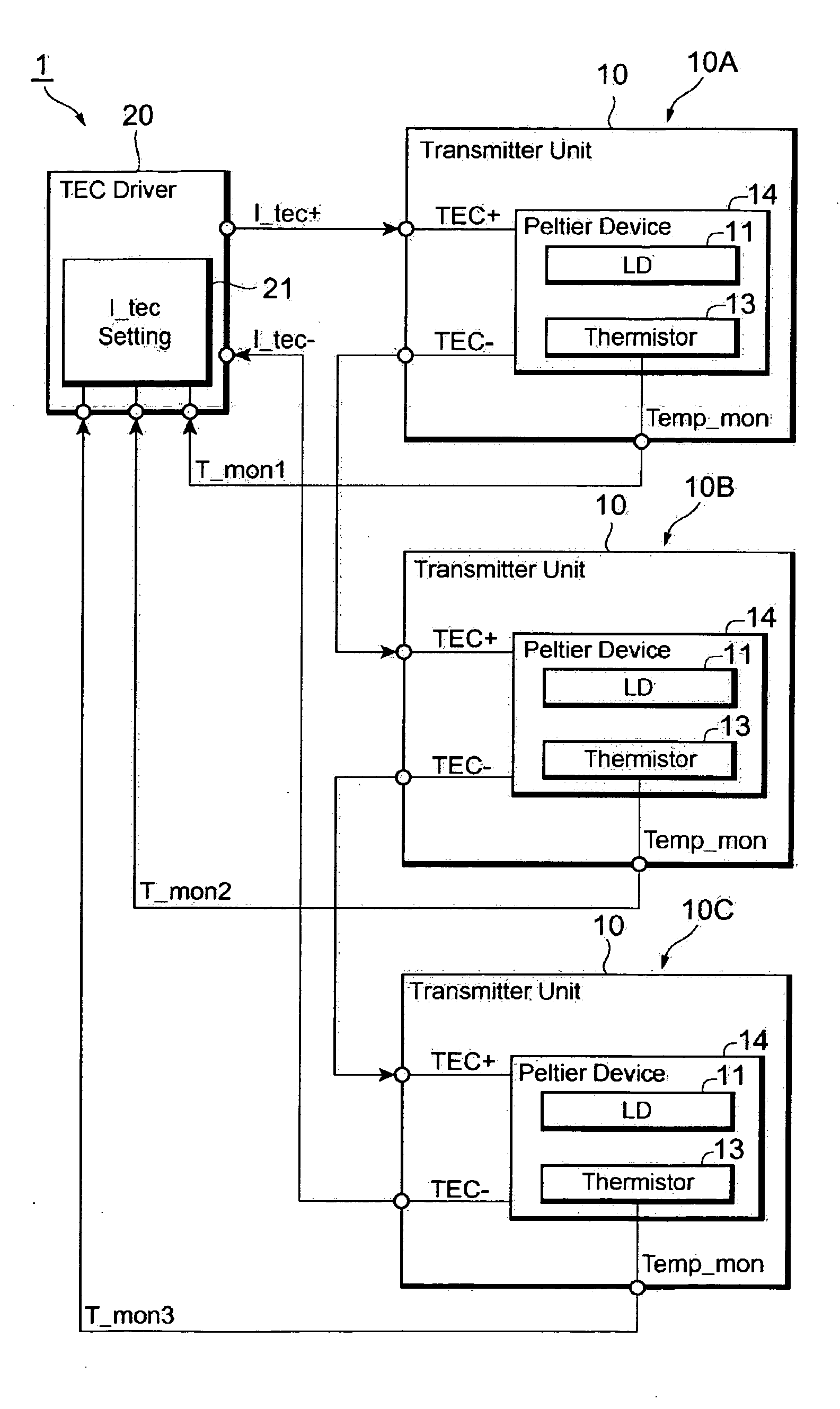
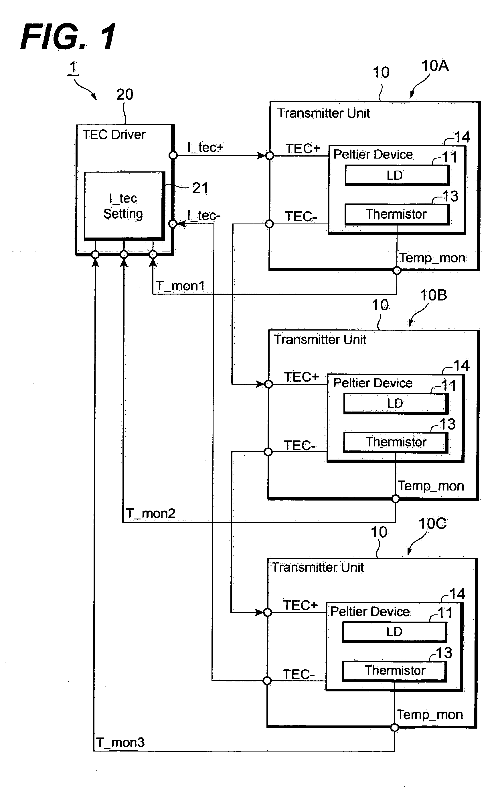
[0015]FIG. 1 schematically illustrates a block diagram of an optical transmitter according to the first embodiment of the invention. The optical transmitter 1, which is installed in a optical communication system for the wavelength division multiplexing (WDM) standard, comprises a plurality of transmitter units 10, three units, 10A to 10C are illustrated in FIG. 1, and a TEC driver 20. Each transmitter unit, 10A to 10C, includes a laser diode (hereafter denoted as LD) 11, a Peltier device 14 and a thermistor 13. The LD 11 emits signal light with a wavelength specific to the transmitter unit by supplying a current from an LD driver, which is not shown in FIG. 1.

[0016]The transmitter unit 10 provides a Peltier device 14 that heats up or cools down a temperature of the LD 11 by receiving a driving current from the TEC driver 20. Peltier devices 14 in each transmitter units, 10A to 10C, are connected in series with respect to the TEC driver 20. That is, one current input terminal TEC+ o...

second embodiment

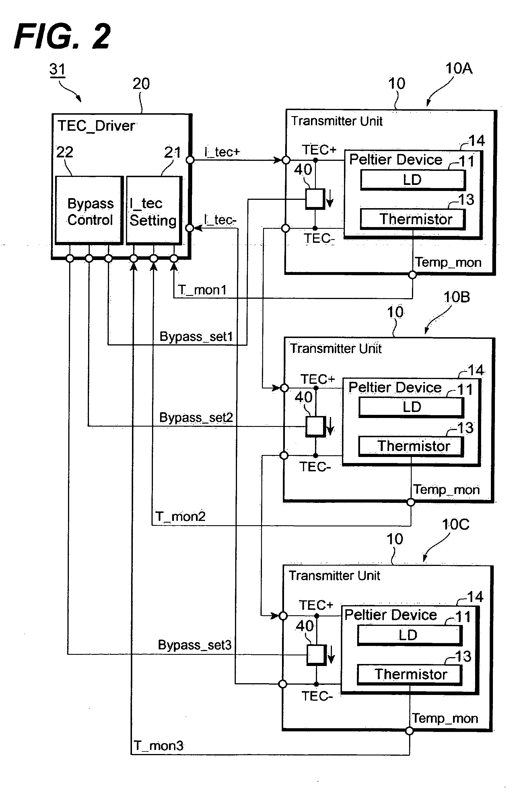
[0021]Next, another embodiment according to the present invention will be described. FIG. 2 schematically illustrates a block diagram of an optical transmitter 31 of the second embodiment of the invention. The optical transmitter 31 has a feature that each transmitter unit 10A to 10C provides a bypassing unit 40. That is, the bypassing unit 40 in each transmitter unit 10 is connected in parallel to the transmitter unit such that the driving current is bypassed from the Peltier device 14 in the transmitter unit 10. Moreover, the TEC driver 20 further provides a bypass control unit 22.

[0022]The bypassing unit 40, as shown in FIG. 3, provides a switching device 41, a resistive element 42, and a pair of low-passing filters, 43 and 44. The switching device 41 may be an active device, such as power MOSFET, whose conductive state is controlled by the signal, Bypass_set_n, output from the TEC driver 20. The duration of ON state of this switching device 41 may be finely adjustable by the pro...


PUM


Abstract

In a semiconductor laser manufacturing method, a GaN single-crystal substrate is formed by slicing a GaN bulk crystal, grown on a c-plane, parallel to an a-plane which is perpendicular to the c-plane. In this substrate, crystal defects extending parallel to the c-axis direction do not readily exert an influence, and degradation of element characteristics due to crystal defects can be suppressed. Further, because the a-plane is a nonpolar plane, improved light emission efficiency and longer wavelengths can be achieved compared with the c-plane, which is a polar plane. Hence a semiconductor laser manufacturing method of this invention enables further improvement of the element characteristics of the semiconductor laser to be fabricated.

Description

BACKGROUND OF THE INVENTION[0001]1. Field of the Invention[0002]The present invention relates to an optical transmitter with a plurality of transmitter units each emitting signal light with specific wavelengths controlled by adjusting a temperature of a semiconductor laser diode.[0003]2. Related Background Art[0004]Some optical transmitter applied in the wavelength division multiplexing (WDM) communication system installs a plurality of optical transmitter units each emitting signal light whose wavelength is specific to one of the signal channels in the WDM system. Such a transmitter unit often provides a Peltier device to adjust a temperature of the semiconductor laser diode (hereafter denoted as LD) in the target temperature. The United States Patents issued as U.S. Pat. No. 5,515,682 and U.S. Pat. No. 5,920,583, and Japanese Patent Application published as JP-H10-141781 have disclosed a driver circuit to control such Peltier devices. However, when the transmitter provides a plura...

Claims


Application Information

Patent Timeline
Patent Type & Authority Applications(United States)
IPC IPC(8): H01S3/10H01S3/04H01S5/024H04B10/40H04B10/07H04B10/50H04B10/60
CPCH01S5/024H01S5/4031H01S5/0612H01S5/02415
Inventor FUNADA, TOMOYUKI
Owner SUMITOMO ELECTRIC IND LTD
Why Eureka
Try Eureka