Method for fabricating recess gate in semiconductor device

Inactive Publication Date: 2009-04-02
SK HYNIX INC
View PDF4 Cites 161 Cited by
  • Summary
  • Abstract
  • Description
  • Claims
  • Application Information

AI Technical Summary

Benefits of technology

[0016]Embodiments of the present invention are directed to providing a method for fabricating a recess gate in a semiconductor

Problems solved by technology

However, the channel length decreases due to a reduction in the pattern size and the electric field increases due to an increase in the ion implant doping concentration of the substrate, thus causing a junction leakage.
This makes it

Method used


Image

  • Method for fabricating recess gate in semiconductor device
  • Method for fabricating recess gate in semiconductor device
  • Method for fabricating recess gate in semiconductor device

Examples


Embodiment Construction

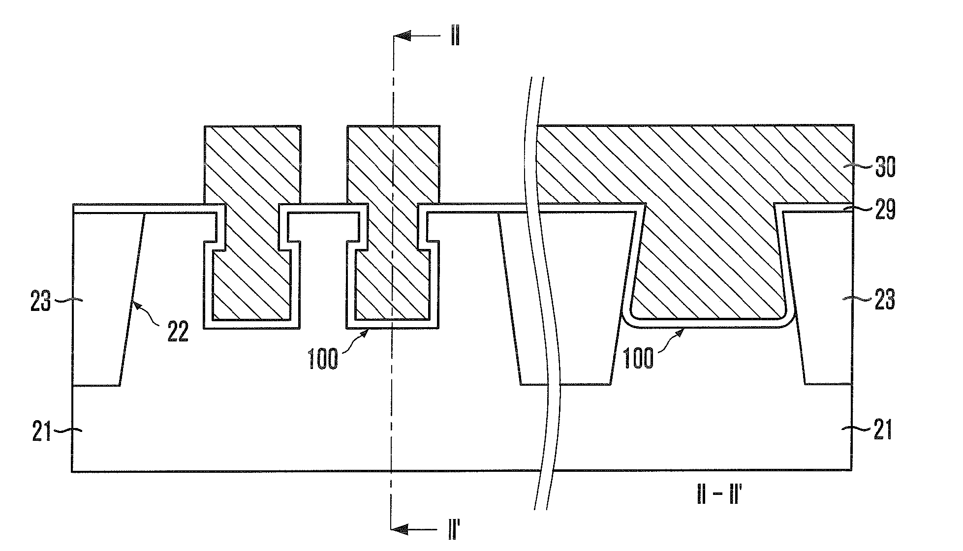
[0027]Hereinafter, a method for fabricating a recess gate in a semiconductor device in accordance with the present invention will be described in detail with reference to the accompanying drawings.

[0028]It will be understood that when an element such as a layer, a film, a pattern and a region is referred to as being ‘on / under’ another element herein, it may be directly on / under the other element, and one or more intervening elements may also be present.

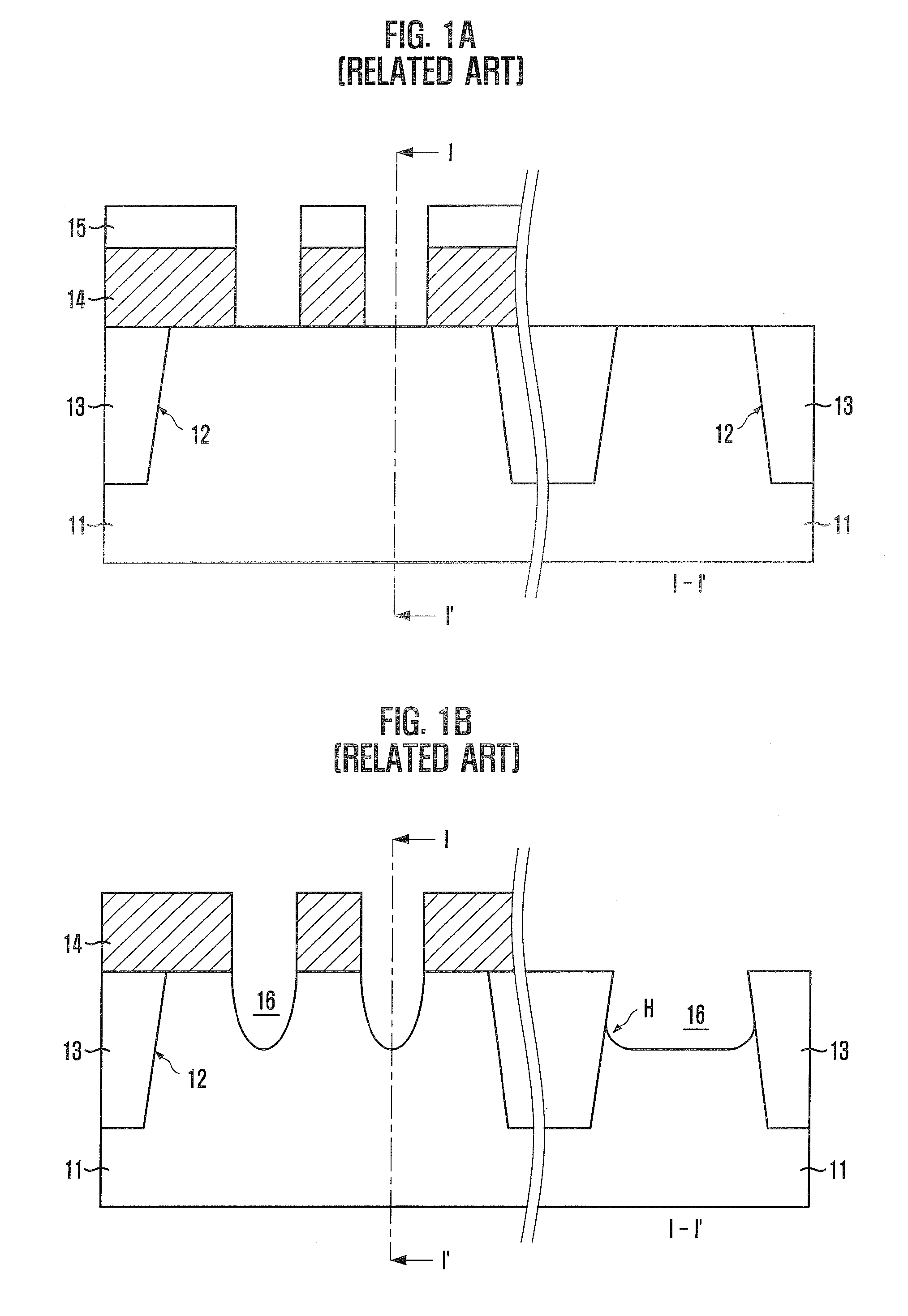
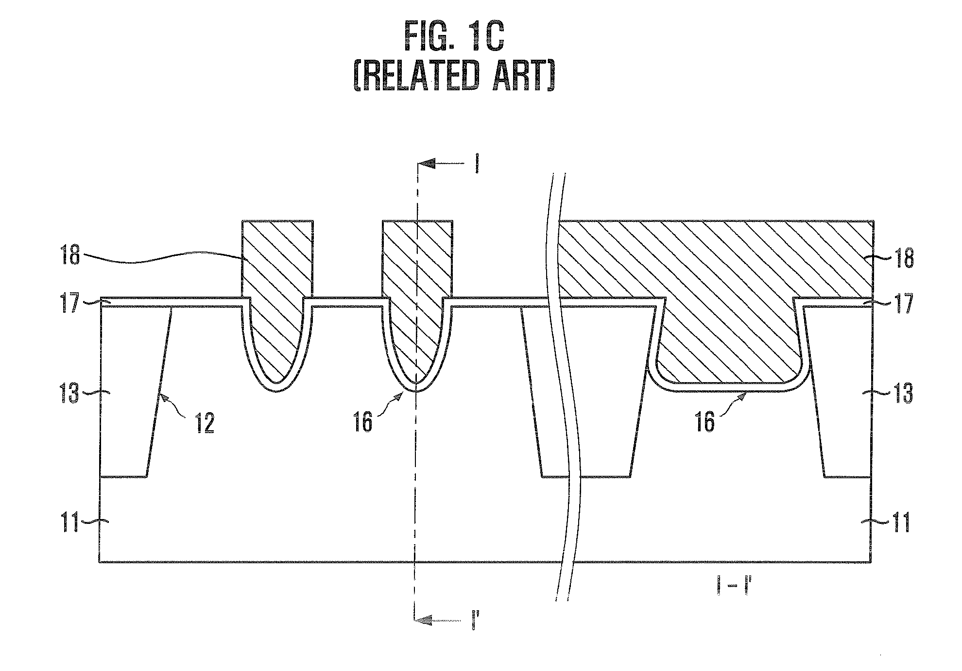
[0029]In the embodiments of the present invention, a hard mask layer with a stack of a passivation layer, e.g., an oxide layer, and an amorphous carbon layer is used as an etch barrier in a recess etching process for forming a recess region or a recess channel. The recess etching process includes a first recess etching process using an amorphous carbon layer as an etch barrier and a second recess etching process using a passivation layer as an etch barrier. The first recess etching process and the second recess etching process are per...


PUM


Abstract

A method for fabricating a recess gate in a semiconductor device includes etching a silicon substrate to form a trench that defines an active region, forming a device isolation layer that gap-fills the trench, forming a hard mask layer over the silicon substrate, the hard mask layer comprising a stack of an oxide layer and an amorphous carbon layer, wherein the hard mask layer exposes a channel target region of the active region, and forming a recess region with a dual profile by first etching and second etching the channel target region using the hard mask layer as an etch barrier, wherein the second etching is performed after removing the amorphous carbon layer.

Description

CROSS-REFERENCE TO RELATED APPLICATIONS[0001]The present invention claims priority of Korean patent application number 2007-0098221, filed on Sep. 28, 2007, which is incorporated by reference in its entirety.BACKGROUND OF THE INVENTION[0002]The present invention relates to semiconductor device fabrication, and more particularly, to a method for fabricating a recess gate in a semiconductor device.[0003]In the fabrication of a semiconductor device, a planar gate forming method is used to form a gate on a planar active region. However, the channel length decreases due to a reduction in the pattern size and the electric field increases due to an increase in the ion implant doping concentration of the substrate, thus causing a junction leakage. This makes it difficult to obtain the refresh characteristics of the device.[0004]In order to solve the above limitation, a three-dimensional recess gate process has been proposed as an alternative gate forming method that forms a gate after etchi...

Claims


Application Information

Patent Timeline
IPC IPC(8): H01L21/76H01L21/302
CPCH01L21/28114H01L29/66621H01L29/42372H01L29/4236H01L21/76224H01L29/1037
Inventor CHO, YONG-TAEKIM, EUN-MI
Owner SK HYNIX INC
Why Eureka
Try Eureka