

Epitaxial substrate and manufacturing method thereof and manufacturing method of light emitting diode apparatus
- Summary
- Abstract
- Description
- Claims
- Application Information
AI Technical Summary
Benefits of technology
Problems solved by technology
Method used
Image

Examples
first embodiment
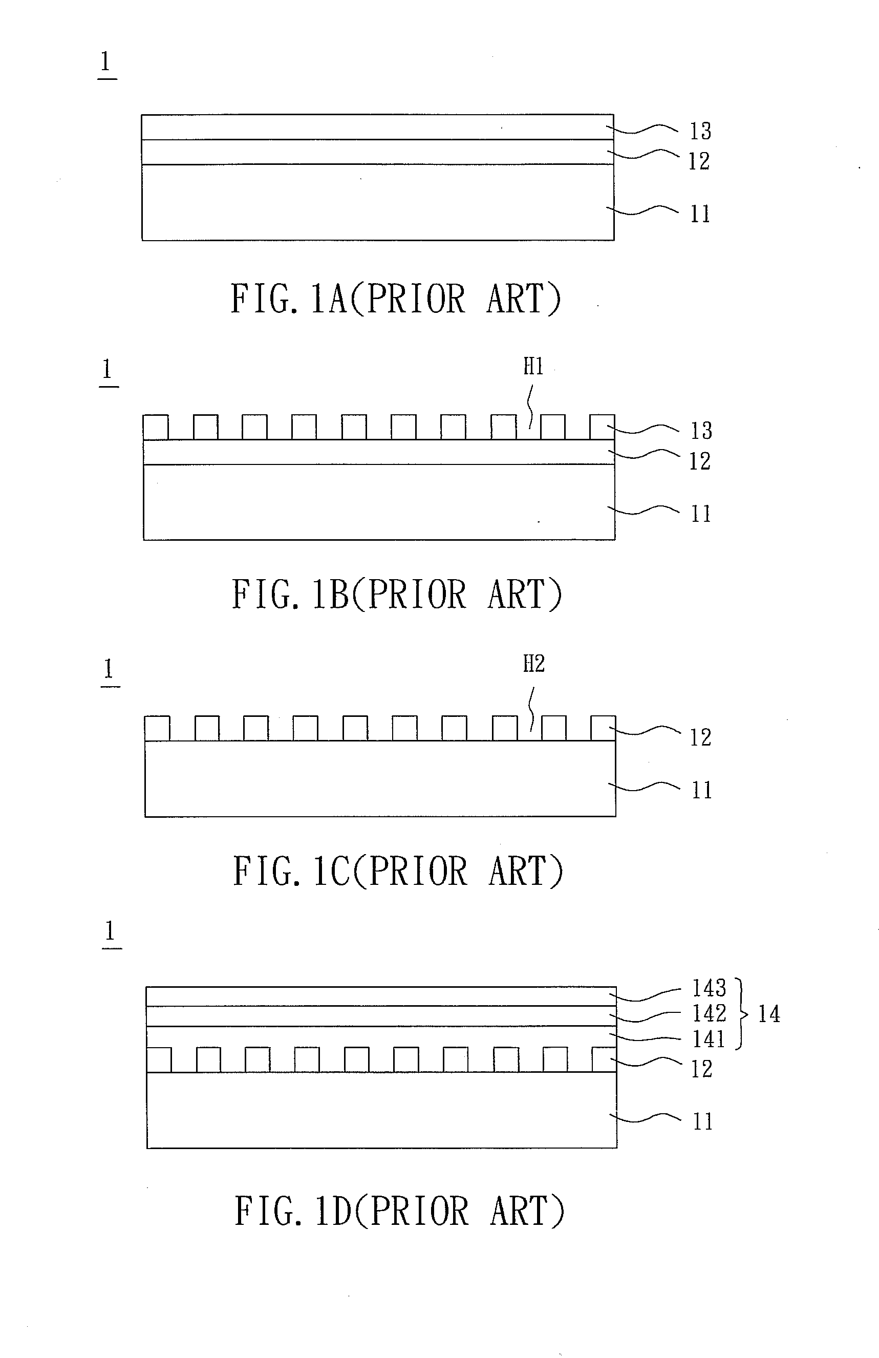
[0031]Referring to FIG. 2, a manufacturing method of an epitaxial substrate according to the present invention includes steps S11 to S13. Illustrations will be made with reference to FIGS. 2 and 3A to 3C.
[0032]As shown in FIG. 3A, a sacrificial layer 22 is formed on a substrate 21 in the step S11. In this embodiment, the sacrificial layer 22 is formed by mixing metal oxide 221 and a plurality of micro / nano particles 222 with the properly adjusted ratio so that the micro / nano particles 222 are periodically arranged in the metal oxide 221.
[0033]The material of the micro / nano particle 222 includes metal, dielectric material, organic material or inorganic material. The micro / nano particle 222 may be a nano-ball, a nano-column, a nano-hole, a nano-point, a nano-line or a nano-concave-convex structure. Herein, the micro / nano particle 222 is the nano-ball, and the material of the metal oxide 221 includes aluminum oxide.
[0034]As shown in FIG. 3B, the micro / nano particle 222 is removed by et...
second embodiment
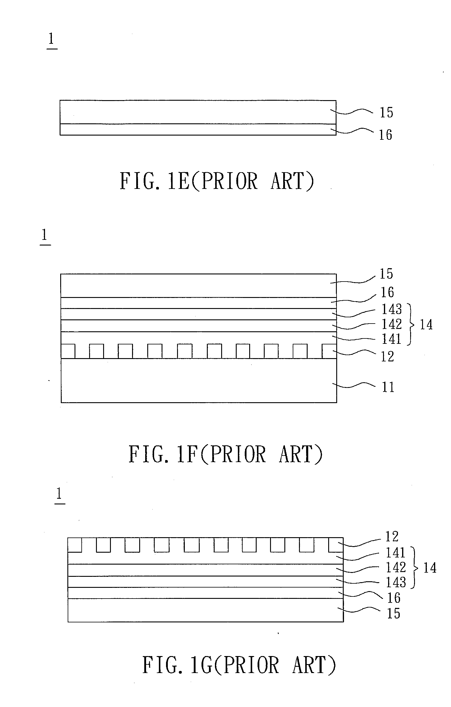
[0036]As shown in FIG. 4, a manufacturing method of an epitaxial substrate according to the present invention includes steps S21 to S25. Illustrations will be made with reference to FIGS. 4 and 5A to 5E.
[0037]As shown in FIG. 5A, a sacrificial layer 32 is formed on a substrate 31 in the step S21. Herein, the sacrificial layer 32 has a first micro / nano structure. The first micro / nano structure is formed by stacking, sintering, anode aluminum oxide (AAO) processing, nano-imprinting, transfer printing, hot pressing, etching or electron beam writer (E-beam writer) processing.
[0038]In this embodiment, the first micro / nano structure has a plurality of micro / nano particles including at least one nano-ball, nano-column, nano-hole, nano-point, nano-line or nano-concave-convex structure. Herein, the first micro / nano structure is the nano-ball, and the material of the micro / nano particle may include metal, dielectric material, organic material or inorganic material. The micro / nano particles ar...
third embodiment
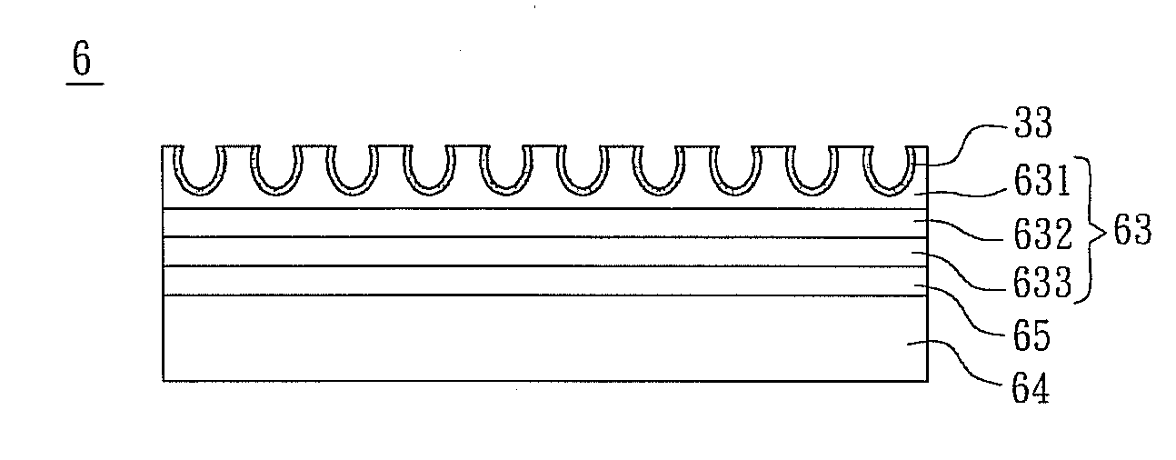
[0045]As shown in FIG. 6, a manufacturing method of an epitaxial substrate according to the present invention includes steps S31 to S36. Illustrations will be made with reference to FIGS. 6 and 7A to 7F.
[0046]As shown in FIG. 7A, a buffer layer 42 is formed on a substrate 41 in the step S31. In this embodiment, the material of the buffer layer 42 can be aluminum nitride or gallium nitride.
[0047]As shown in FIG. 7B, a sacrificial layer 43 is formed on a buffer layer 43 in the step S32. In this embodiment, the sacrificial layer 43 has a first micro / nano structure, which is manufactured by stacking, sintering, anode aluminum oxide processing, nano-imprinting, transfer printing, hot pressing, etching or electron beam exposure.
[0048]Herein, the first micro / nano structure has a plurality of micro / nano particles including at least one nano-ball, a nano-column, a nano-hole, a nano-point, a nano-line or a nano-concave-convex structure. In this embodiment, the first micro / nano structure is th...
PUM
 Abstract
Description
Claims
Application Information