LED device having improved light output

Active Publication Date: 2009-04-09
GLOBAL OLED TECH
View PDF13 Cites 94 Cited by
  • Summary
  • Abstract
  • Description
  • Claims
  • Application Information

AI Technical Summary

Benefits of technology

[0014]The present invention has the advantage that it increases the

Problems solved by technology

Because LED devices employ high-optical-index emissive materials, a large fraction (e.g. greater than 50%) of the emitted light is trapped in the device due to total internal reflection and thus reduces the device efficiency.
While such designs are useful, they require a patterned organic material deposition technology (for example, vacuum deposition through metal shadow-masks) that is difficult to scale to large substrates.
Moreover, optical cavity devices typically suffer from an unacceptable angular color dependence.
However, while useful, such an approach does not improve the manufacturability of the device and provides inadequate ambient contrast ratio under some illumination conditions.
Moreover, the color filters absorb light emitted from the light-emitting layer, thereby reducing device efficiency.
Such designs, however, may have increased manufacturing costs, lower light output than desired, and reflectance larger than may be d

Method used


Image

  • LED device having improved light output
  • LED device having improved light output
  • LED device having improved light output

Examples


Example

[0030]It will be understood that the figures are not to scale since the individual layers are too thin and the thickness differences of various layers too great to permit depiction to scale.

DETAILED DESCRIPTION OF THE INVENTION

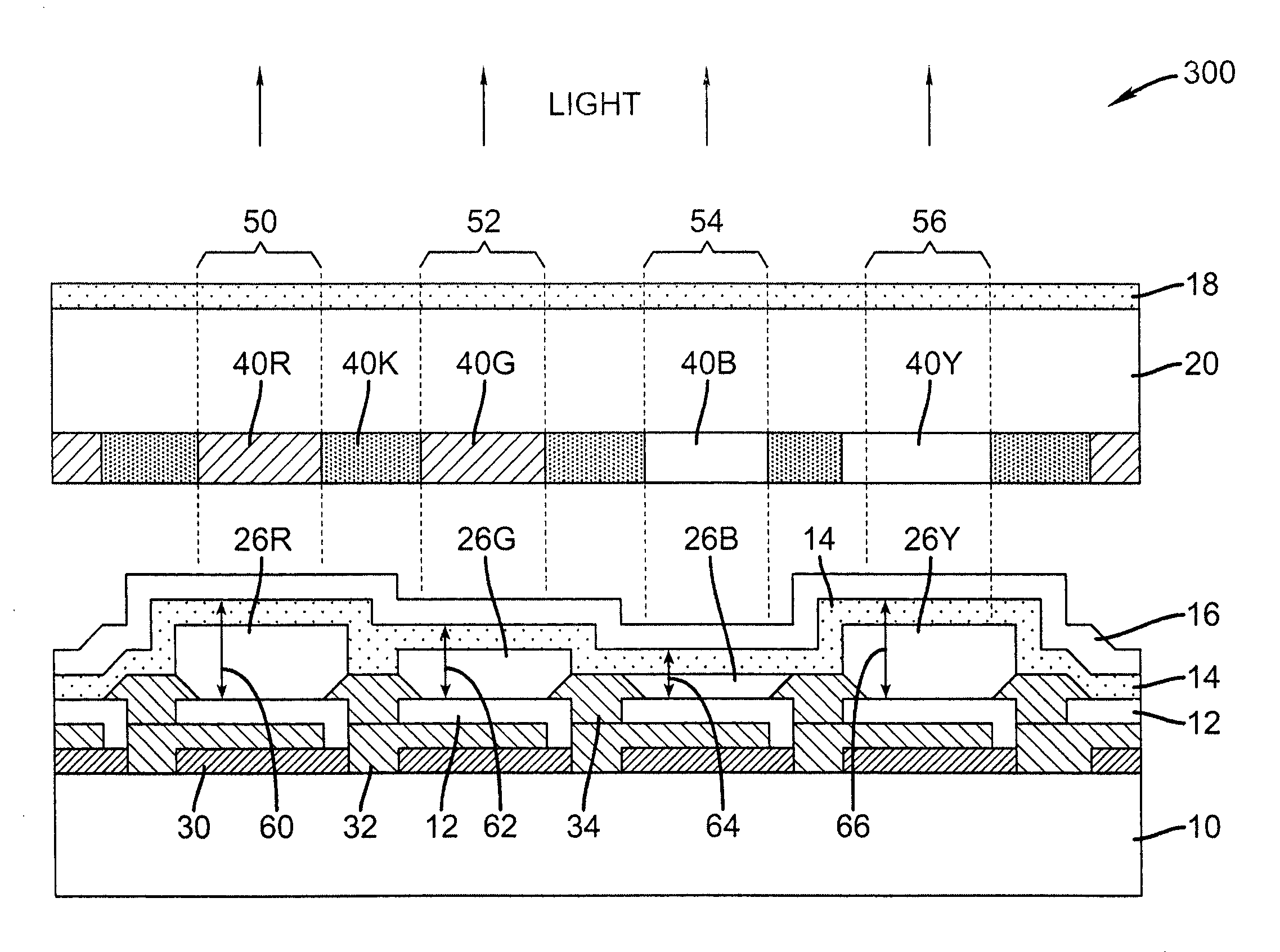
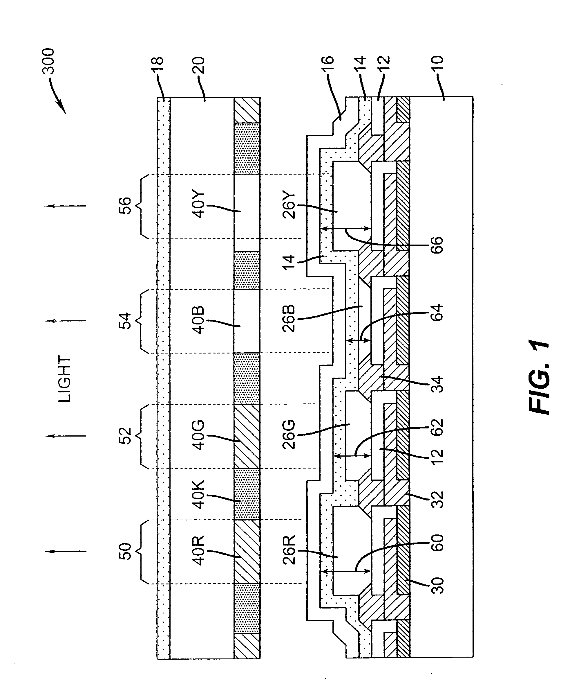
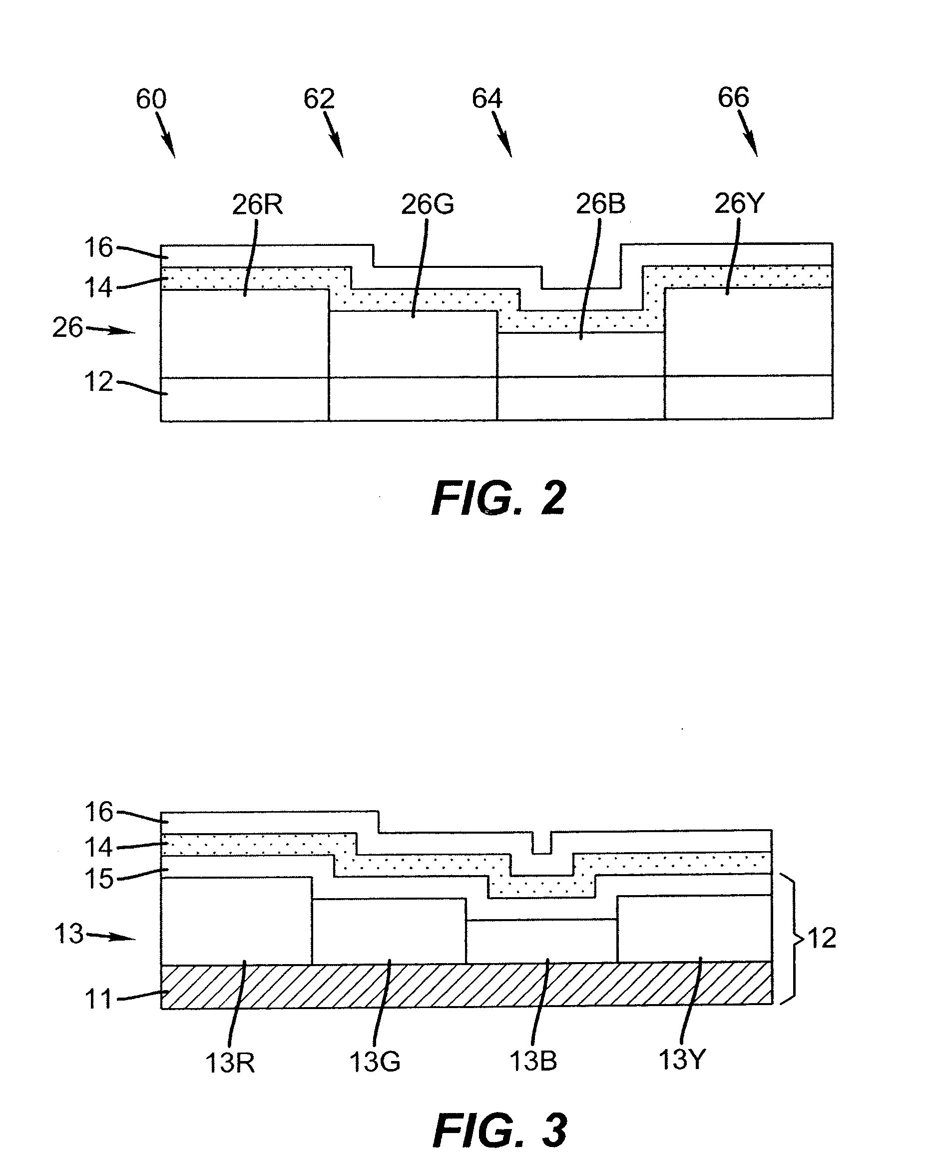
[0031]Referring to FIG. 1, an exemplary embodiment of a light-emitting diode device according to the present invention comprises a substrate 10, a reflective electrode 12, and a semi-transparent electrode 16 formed over the substrate 10. Either the reflective electrodes 12 or semi-transparent electrodes 16 are patterned to form a plurality of independently-controllable light-emitting sub-pixel elements 50, 52, 54, and 56. As shown in FIG. 1, for example, reflective electrode 12 is patterned. The independently-controllable light-emitting elements can be controlled, for example by thin-film electronic components 30 formed on the substrate 10. The other electrode (e.g. 16) can be unpatterned and electrically common to all of the light-emitting elements 50, 52, 54...


PUM


Abstract

A light-emitting microcavity diode device includes a reflective electrode and a semi-transparent electrode, formed over a substrate, with an unpatterned light-emitting layer formed between the reflective electrode and the semi-transparent electrode. The reflective electrode, semi-transparent electrode, and unpatterned light-emitting layer form an optical cavity. Either the reflective or semi-transparent electrode is patterned to form independently-controllable, light-emitting sub-pixels. At least one, and fewer than all, of the sub-pixels emit light through a color filter. A first sub-pixel emits light having a first primary color and a second sub-pixel emits a complementary colored light. The light emitted from the first and second sub-pixels changes at one or more different angles. The color of the combined light of the first and second sub-pixels changes less at the one or more different angles than the light from at least one of the first or second sub-pixels. A third sub-pixel emits light through a color filter of a second primary color, different from the first primary color.

Description

FIELD OF THE INVENTION[0001]The present invention relates to light-emitting diode (LED) devices, and more particularly, to LED device structures for improving light output efficiency.BACKGROUND OF THE INVENTION[0002]Emissive flat-panel display devices are widely used in conjunction with computing devices and in particular with portable devices. These displays are often used in public areas with significant ambient illumination and are viewed from a wide variety of angles.[0003]Light emitting diodes (LED) incorporating thin films of light-emitting materials have many advantages in a flat-panel display device and are useful in optical systems. U.S. Pat. No. 6,384,529 issued May 7, 2002 to Tang et al. shows an OLED color display that includes an array of organic LED light-emitting elements (pixels). Light is emitted from a pixel when a current is passed through an organic material, the frequency of the light is dependent on the nature of the organic material used. The organic materials...

Claims


Application Information

Patent Timeline
IPC IPC(8): H01J1/62H01J9/02
CPCH01L27/3213H01L51/5284H01L51/5265H01L27/322H10K59/30H10K59/351H10K59/38H10K50/852H10K50/865
Inventor COK, RONALD S.MILLER, MICHAEL E.
Owner GLOBAL OLED TECH
Why Eureka
Try Eureka