Hole-injecting layer in oleds

a technology of oleds and holes, applied in the direction of discharge tubes/lamp details, discharge tubes luminescnet screens, organic semiconductor devices, etc., can solve the problems of high drive voltage, low operational life, and inability to effectively use anodes as-prepared or cleaned

Inactive Publication Date: 2009-04-09
GLOBAL OLED TECH
View PDF99 Cites 30 Cited by
  • Summary
  • Abstract
  • Description
  • Claims
  • Application Information

AI Technical Summary

Problems solved by technology

However, the as-prepared or clean ITO cannot be used as an effective anode because of its relatively low work function.
The low work function anode will form a high barrier for holes to inject from the anode into the adjacent organic EL unit, resulting in high drive voltage and low operational lifetime.
However, the improved EL performance is not effective enough for practical applications.
However, the aforementioned HIL's described by the prior art (with its HOMO level close to the work function of the anode) are not stable.
An OLED having this type of HIL usually has high voltage rise during operation, resulting in inferior performance.
If an OLED has high voltage rise during operation using the constant voltage mode, the given current will likewise decrease because the constant voltage mode cannot provide increased voltage to keep the given current unchanged.
Moreover, in most cases, there is a voltage limitation in the drive circuitry, especially for low cost

Method used


Image

  • Hole-injecting layer in oleds
  • Hole-injecting layer in oleds
  • Hole-injecting layer in oleds

Examples


example 2 (

Inventive)

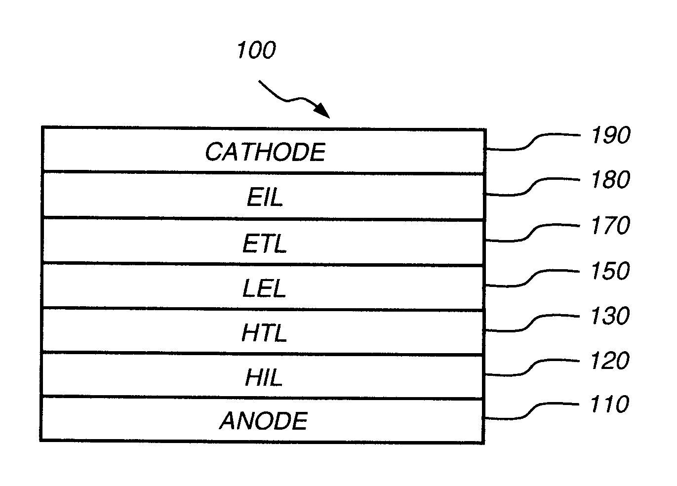
[0231]Another OLED (Device 2) which is fabricated with the same method and the same layer structure as Example 1, except that an HIL is inserted between the modified ITO anode and the HTL. The layer structure is:

[0232]a) an HIL, 55 nm thick, including hexaazatriphenylene hexacarbonitrile (HAT-CN) doped with 5% by volume of 4,4′,4″-tris[(3-ethylphenyl)phenylamino]triphenylamine (m-TDATA), wherein the reduction potential of HAT-CN is −0.08 V vs. SCE (greater than −0.1 V vs. SCE) and the oxidation potential of m-TDATA is 0.46 V (less than 1.0 V vs. SCE);

[0233]b) a HTL, 20 nm thick, including NPB;

[0234]c) a LEL, 30 nm thick, including Alq doped with 1.0% by volume of C545T;

[0235]d) an ETL, 30 nm thick, including Alq doped with 1.5% by volume of Li, which is also considered as an EIL; and

[0236]e) a cathode: approximately 210 nm thick, including MgAg.

[0237]Device 2 is denoted as: ITO / 55 nm (HAT-CN):5%(m-TDATA) / 20 nm NPB / 30 nm Alq:1.0% C545T / 30 nm Alq:1.5% Li / 210 nm MgAg. The EL ...

example 7 (

Inventive)

[0269]An inventive OLED (Device 7) is fabricated with the same method and the same layer structure as Example 6, except that the HIL includes a first material and a second material. The layer structure is:

[0270]a) an HIL, 55 nm thick, including HAT-CN doped with 5% by volume of Formula Inv-1, wherein the reduction potential of HAT-CN is −0.08 V vs. SCE (greater than −0.1 V vs. SCE) and the oxidation potential of Formula Inv-1 is 0.68 V (less than 1.0 V vs. SCE);

[0271]b) a HTL, 20 nm thick, including NPB;

[0272]c) a LEL, 30 nm thick, including Alq doped with 1.0% by volume of C545T;

[0273]d) an ETL, 30 nm thick, including Alq doped with 1.2% by volume of Li, which is also considered as an EIL; and

[0274]e) a cathode: approximately 210 nm thick, including MgAg.

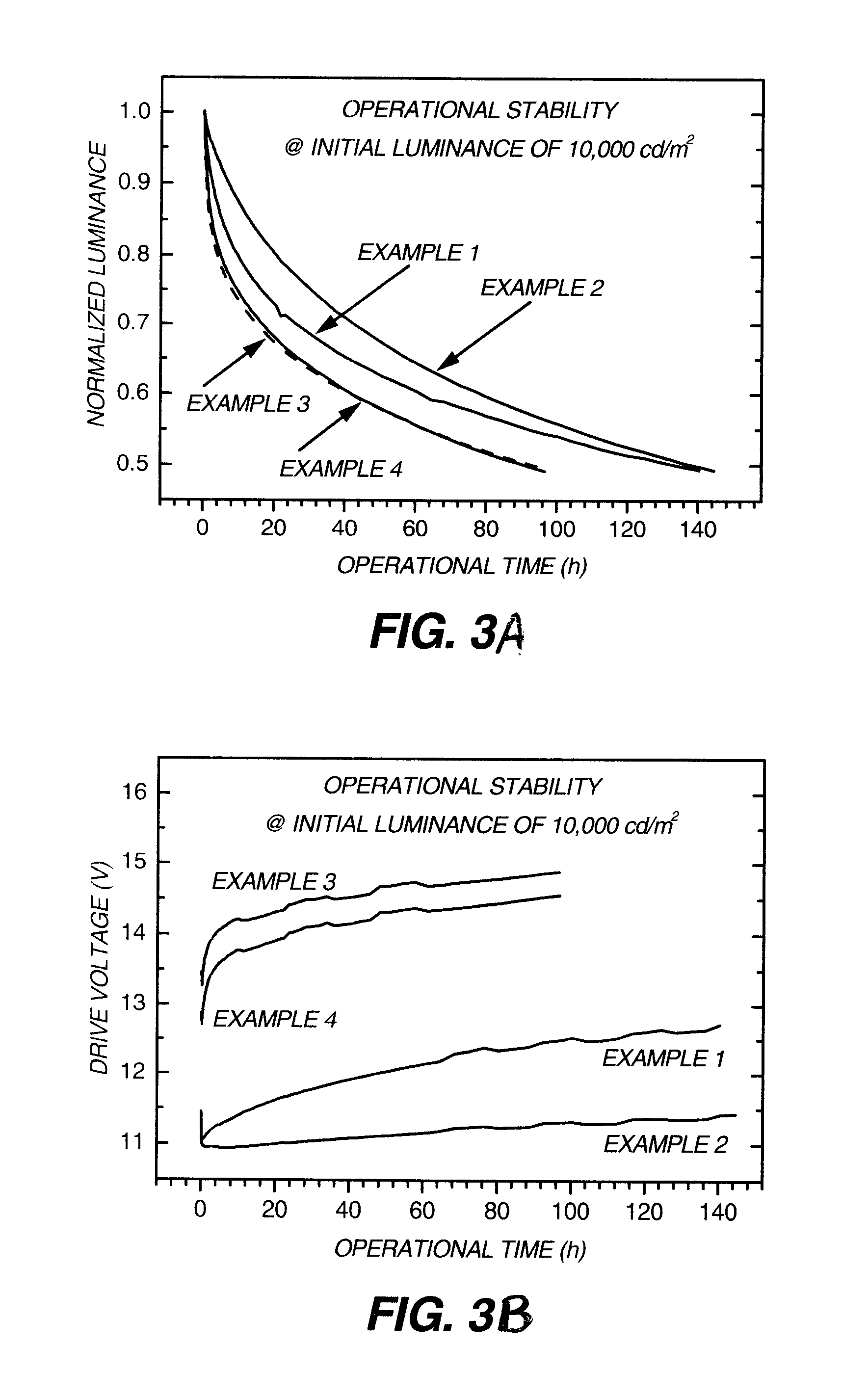
[0275]Device 7 is denoted as: ITO / 55 nm (HAT-CN):5% (Formula Inv-1) / 20 nm NPB / 30 nm Alq:1.0% C545T / 30 nm Alq:1.2% Li / 210 m MgAg. The EL performance of the device is summarized in Table 4, and its operational stability is ...

example 8 (

Inventive)

[0276]An inventive OLED (Device 8) is fabricated with the same method and the same layer structure as Example 7, except that the thickness of HIL is increased. The layer structure is:

[0277]a) an HIL, 130 nm thick, including HAT-CN doped with 5% by volume of Formula Inv-1;

[0278]b) an HTL, 20 nm thick, including NPB;

[0279]c) an LEL, 30 nm thick, including Alq doped with 1.0% by volume of C545T;

[0280]d) an ETL, 30 nm thick, including Alq doped with 1.2% by volume of Li, which is also considered as an EIL; and

[0281]e) a cathode: approximately 210 nm thick, including MgAg.

[0282]Device 8 is denoted as: ITO / 130 nm (HAT-CN):5% (Formula Inv-1) / 20 nm NPB / 30 nm Alq:1.0% C545T / 30 nm Alq:1.2% Li / 210 nm MgAg. The EL performance of the device is summarized in Table 4, and its operational stability is shown in FIGS. 4A and 4B.


PUM


Abstract

An OLED including an anode; a cathode; a hole-injecting layer disposed over the anode, wherein the hole-injecting layer includes a first organic material with a reduction potential greater than −0.1 V and a lesser amount by volume of a second material with an oxidation potential less than 0.7 V, and wherein the second material does not include metal complexes; a hole-transporting layer disposed over the hole-injecting layer; a light-emitting layer disposed between the hole-transporting layer and the cathode; and an electron-transporting layer disposed between the light-emitting layer and the cathode.

Description

CROSS REFERENCE TO RELATED APPLICATION[0001]Reference is made to commonly assigned U.S. patent application Ser. No. 11 / 301,458 filed Dec. 13, 2005, by Kevin P. Klubek et al., entitled “Electroluminescent Device Containing An Anthracene Derivative”, the disclosure of which is herein incorporated by reference.FIELD OF INVENTION[0002]The present invention relates to organic light-emitting devices (OLEDs) or organic electroluminescent (EL) devices having an improved hole-injecting layer.BACKGROUND OF THE INVENTION[0003]Multiple-layered OLEDs or organic EL devices, as first described by Tang in commonly assigned U.S. Pat. No. 4,356,429, are used as color pixel components in OLED displays and as solid-state lighting sources. OLEDs are also useful for some other applications due to their low drive voltage, high luminance, wide viewing angle, fast signal response time, and simple fabrication process.[0004]A typical OLED includes two electrodes and one organic EL unit disposed between the tw...

Claims


Application Information

Patent Timeline
IPC IPC(8): H01L51/52
CPCH01L51/006H01L51/0072H01L2251/554H01L51/5088H01L51/0081H10K85/633H10K85/6572H10K85/324H10K50/17H10K2101/50
Inventor LIAO, LIANG-SHENGKLUBEK, KEVIN P.
Owner GLOBAL OLED TECH
Why Eureka
Try Eureka