Plating method

Inactive Publication Date: 2009-04-16
EBARA CORP +1
View PDF8 Cites 12 Cited by
  • Summary
  • Abstract
  • Description
  • Claims
  • Application Information

AI Technical Summary

Benefits of technology

[0024]The plating method of the present invention makes it possible to easily correct a thickness profile of a plated film simply by adjusting the current applied to the auxiliary cathode. This enables a lower-cost and flexible apparatus operation in a semiconductor device manufacturing process. Furth

Problems solved by technology

This impedes electrode position of copper in the trenches 4 and contact holes 3 in the next plating step, whereby voids are likely to be formed within the interconnects formed of a plated film, lowering the reliability of the interconnects.
When carrying out CMP or the lik

Method used


Image

  • Plating method
  • Plating method
  • Plating method

Examples


Example

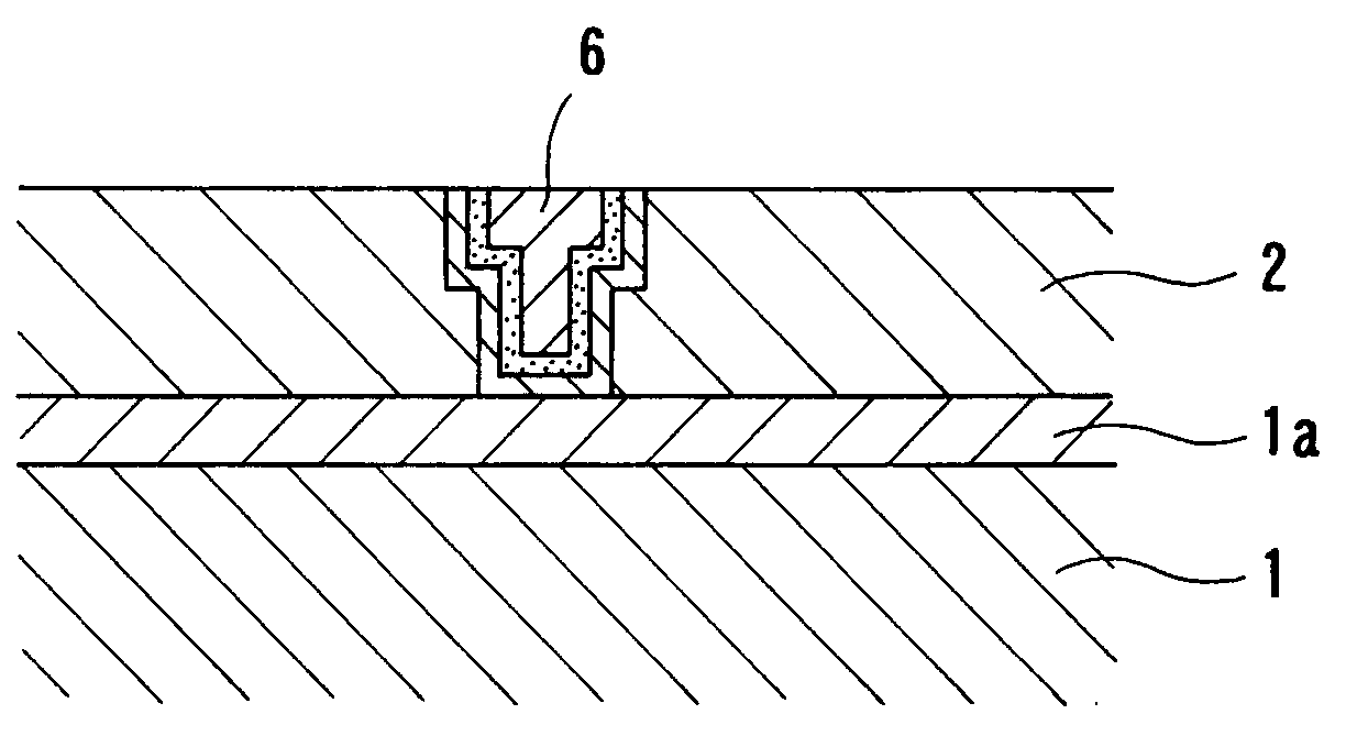
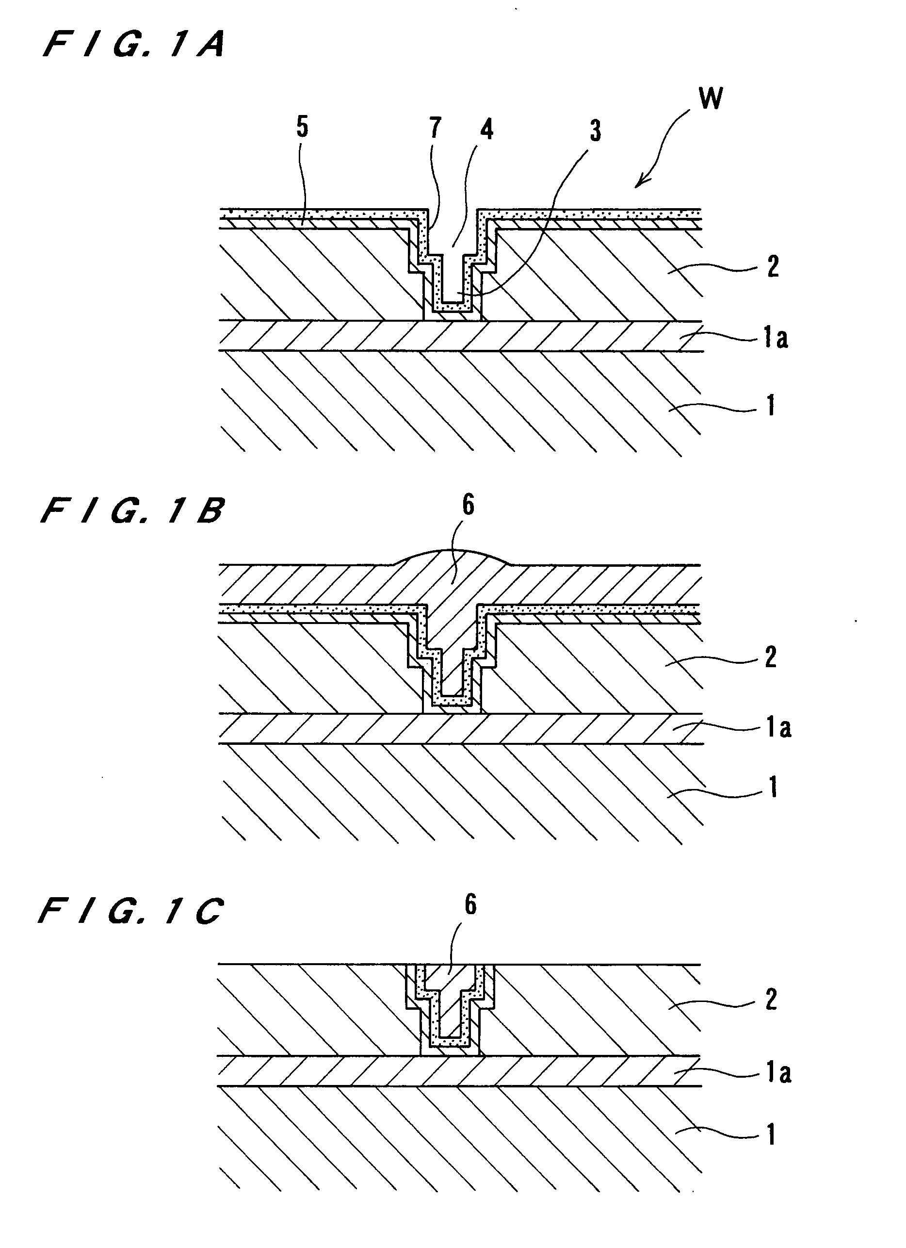
[0045]Preferred embodiments of the present invention will now be described in detail with reference to the drawings. The following embodiments relate to the application of the present invention useful for forming interconnects of copper by filling copper into interconnect recesses, such as contact holes 3 and trenches 4, formed in a insulating film 2 by plating onto a surface of a seed layer 7 as a conductive film having formed on the surface of the substrate W, as shown in FIGS. 1A and 1B.

[0046]FIG. 7 is an overall plan view of a substrate processing apparatus incorporating a plating apparatus for performing a plating method of the present invention. As shown in FIG. 7, this substrate processing apparatus has a facility which houses therein two loading / unloading units 10 for housing a plurality of substrates W therein, two plating apparatuses 12 for performing a plating process and processing incidental thereto, a transfer robot 14 for transferring substrates W between the loading / ...


PUM


Abstract

A plating method can form a plated film having a uniform thickness over the entire surface, including the peripheral surface, of a substrate. The plating method includes: disposing an anode so as to face a conductive film, formed on a substrate, which serves as a cathode, and disposing an auxiliary cathode on an ring-shaped seal member for sealing a peripheral portion of the substrate; bringing the conductive film, the anode and the auxiliary cathode into contact with a plating solution; and supplying electric currents between the anode and the conductive film, and between the anode and the auxiliary cathode to carry out plating.

Description

BACKGROUND OF THE INVENTION[0001]1. Field of the Invention[0002]The present invention relates to a plating method, and more particularly to a plating method used for filling interconnect recesses formed in a surface of a substrate, such as a semiconductor wafer, with an electrical conductor (interconnect material), such as copper or silver, so as to form interconnects.[0003]2. Description of the Related Art[0004]In recent years, instead of using aluminum or aluminum alloys as a metallic material for forming interconnect circuits on a semiconductor substrate; there is an eminent movement towards using copper (Cu) that has a low electric resistivity and high electromigration resistance. Copper interconnects are generally formed by filling copper into fine interconnect recesses formed in a surface of a substrate. Various techniques are known for forming such copper interconnects, including CVD, sputtering, and plating. According to any such technique, a copper film is formed in a subst...

Claims


Application Information

Patent Timeline
IPC IPC(8): C25D5/48C25D5/00
CPCC25D17/00C25D21/12C25D17/008H01L21/76877H01L21/2885
Inventor MAKINO, NATSUKINAMIKI, KEISUKEIDE, KUNIHITOKUNISAWA, JUNJIMUSAKA, KATSUYUKIVEREECKEN, PHILIPPEBAKER-O'NEAL, BRETT C.DELIGIANNI, HARIKLIAKWIETNIAK, KEITH
Owner EBARA CORP
Why Eureka
Try Eureka