Semiconductor package and method for fabricating the same

a technology of semiconductor chips and encapsulants, applied in the direction of semiconductor/solid-state device details, semiconductor devices, electrical apparatus, etc., can solve the problems of difficult to efficiently dissipate heat generated from active surfaces of semiconductor chips to external environment via encapsulant, adversely affecting performance and stability, etc., to achieve the effect of dissipating hea

Inactive Publication Date: 2009-04-16
SILICONWARE PRECISION IND CO LTD
View PDF4 Cites 21 Cited by
  • Summary
  • Abstract
  • Description
  • Claims
  • Application Information

AI Technical Summary

Benefits of technology

[0016]In light of the shortcomings of the above prior arts, a primary objective of the present invention is to provide a semiconductor package and a method for fabricating the same, which can dissipate heat and prevent the semiconductor chip from being compressed and damaged during the molding process.
[0017]Another objective of the present invention is to provide a semiconductor package and a method for fabricating the same, which can expose the semiconductor chip without undergoing a polishing process, so as to avoid cracking of the semiconductor chip and reduce the fabrication cost.
[0018]A further objective of the present invention is to provide a semiconductor package and a method for fabricating the same, which can prevent cutting tools from cutting through a heat-dissipating member, thereby avoiding problems such as burr and wearing of the cutting tools during a cutting process so as to reduce the cost of cutting process.
[0024]According to the aforementioned, a semiconductor package is disclosed, comprising: a chip carrier; a semiconductor chip mounted on and electrically connected to the chip carrier; and an encapsulant formed on the chip carrier for encapsulating the semiconductor chip, wherein the encapsulant is formed with a recess corresponding in position to the semiconductor chip so as to expose the semiconductor chip from the encapsulant. Moreover, an interfacial layer or a heat-dissipating member having an interfacial layer may be formed on a surface of the semiconductor chip corresponding in position to the recess of the encapsulant so as to enhance heat dissipation.
[0025]Therefore, as aforementioned, the present invention primarily features in attaching and electrically connecting a semiconductor chip to a chip carrier; forming an interfacial layer or attaching a heat dissipating member having an interfacial layer on the semiconductor chip; forming an encapsulant on the chip carrier for encapsulating the semiconductor chip and the interfacial layer or the heat dissipating member having the interfacial layer, wherein a space is kept between the top surface of the encapsulant and the top surface of the interfacial layer so as to prevent cracking of the semiconductor chip during the molding process; subsequently, cutting the encapsulant along the periphery of the interfacial layer or the periphery of the heat dissipating member having the interfacial layer; and removing the excess or unneeded encapsulant from the interfacial layer so as to dissipate heat and avoid mold flash, wherein the interfacial layer can be left over or removed with the excess encapsulant.
[0026]Accordingly, during fabrication of the present invention, a common polishing process existed in the prior art can be omitted so as to prevent exposing the semiconductor chip to the external environment, thereby avoiding problems such as cracking the semiconductor chip and increasing the cost of production. Moreover, during the cutting process, instead of cutting through the interfacial layer or the heating-dissipating member, the encapsulant of the present invention is cut along the periphery of the interfacial layer or the periphery of the heating-dissipating member, thereby preventing problems such as burr and wearing of cutting tools as well as reducing the cost of the cutting process the heat sink package structure and the method for fabricating the same mainly comprises the steps of mounting and electrically connecting a semiconductor chip to a chip carrier; mounting an interfacial layer or a heat dissipating member having an interfacial layer on the semiconductor chip; forming an encapsulant that encapsulates the semiconductor chip and the interfacial layer or the heat dissipating member having the interfacial layer, wherein a spacing is kept between the top surface of the encapsulant and the interfacial layer so as to prevent cracking of the semiconductor chip during the molding process; subsequently, cutting the encapsulant along edges of the interfacial layer or the heat dissipating member having the interfacial layer; and removing the redundant encapsulant located on the interfacial layer, wherein the interfacial layer can be removed together with the encapsulant thereon or can be left intact. Thus, a heat sink package structure is formed without undergoing a conventional polishing process, thereby avoiding the cracking of the semiconductor chip which may otherwise arise from polishing the encapsulant as taught in the prior art. Since the cutting line does not pass through the heat-dissipating member, the burr problem and wearing of cutting tools can be prevented and thus the cutting cost can be reduced.

Problems solved by technology

However, because such miniaturized but highly integrated packages often produce a surprisingly large amount of heat during operation, it becomes extremely important to find a way to dissipate the heat immediately and efficiently, in order to avoid the heat from being accumulated and adversely affecting performance and stability of semiconductor chips.
Nevertheless, as the encapsulant is made of packaging resin having a remarkably low thermal conductivity around 0.8 w / m-° K, it is quite difficult to efficiently dissipate heat generated from active surfaces of the semiconductor chips to external environment via the encapsulant.
However, if the heat-dissipating member is completely encapsulated by the encapsulant, efficiency of heat dissipation can be hardly improved, because the heat cannot be dissipated without passing through the encapsulant.
Nevertheless, the foregoing semiconductor package 10 and fabrication method thereof have some serious drawbacks.
This thereby adversely affects heat dissipation of the semiconductor chip 11 and appearance of the semiconductor package.
Accordingly, a deflash process has to be performed to remove the mold flash on the top surface of the semiconductor chip 11, thereby increasing the fabrication time and the fabrication cost.
Moreover, the semiconductor package may be easily damaged under the deflash process.
On the other hand, if the summation of the height of the substrate 12 and the semiconductor chip 11 is too high, the semiconductor chip 11 can be easily damaged and cracked because the top surface of the semiconductor chip 11 is abutted to the top wall of the mold cavity 15 with overload stress.
Despite the fact that the polishing process may be costly, the semiconductor chip is often not sufficiently exposed but severely damaged during the polishing process due to warpage of the semiconductor package caused by uneven stress.
In addition, during the polishing process, the semiconductor chip may be easily damaged or cracked by polishing stress.
However, as the heat sink is made of a metal material such as copper and aluminum, employing a cutting tool such as a diamond-cutting tool to cut through the heat sink is likely to form uneven sharp edges (also known as burrs) on the periphery of the heat sink, thereby forming unpleasant outlook of the package and causing severely detritions of the cutting tool as well as increasing cost of production and decreasing yield of production.
Solutions to these problems have been long sought but prior developments have not taught or suggested any solutions, and thus solutions to these problems have long eluded those skilled in the art.

Method used


Image

  • Semiconductor package and method for fabricating the same
  • Semiconductor package and method for fabricating the same
  • Semiconductor package and method for fabricating the same

Examples


first embodiment

[0047]FIGS. 5A to 5D are schematic views showing a semiconductor package capable of dissipating heat, and a method for fabricating the same according to a first embodiment of the present invention.

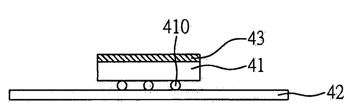
[0048]As shown in FIG. 5A, a semiconductor chip 41 is mounted and electrically connected to a chip carrier 42, wherein an interfacial layer 43 is disposed on a surface of the semiconductor chip 41 that is not attached to the chip carrier 42. The chip carrier 42 may be a ball grid array (BGA) substrate or a land grid array (LGA) substrate. The semiconductor chip 41 may be a flip-chip semiconductor chip having an active surface thereof electrically connected to the chip carrier 42 via a plurality of conductive bumps 410. The interfacial layer 43 may be a polyimide tape (P.I. tape) adhered on the semiconductor chip 41, an epoxy resin applied on the semiconductor chip 41, or an organic layer such as wax formed on the semiconductor chip 41, such that the bonding force between the interfacial la...

second embodiment

[0054]FIGS. 6A to 6C are schematic views showing a semiconductor package capable of dissipating heat, and a method for fabricating the same according to a second embodiment of the present invention. The semiconductor package of the second embodiment is substantially similar to that of the foregoing embodiment. However, one of the major differences between these two embodiments is that a protruding portion is formed on an encapsulant 54 of the second embodiment, so as to facilitate subsequent removal of a portion of the encapsulant 54.

[0055]Referring to FIG. 6A, a molding process is performed, wherein a chip carrier 52 mounted with a semiconductor chip 51 and an interfacial layer 53 is disposed in a mold cavity of a mold (not shown). Moreover, a top portion of the mold cavity further comprises a recessed structure for receiving the packaging resin such that, when an encapsulant 54 encapsulating the semiconductor chip 51 and the interfacial layer 53 is formed, a protruding portion 542...

third embodiment

[0058]FIGS. 7A and 7B are schematic views of a semiconductor package, which is capable of dissipating heat and fabricated according to a third embodiment of the present invention. The semiconductor substrate of the second embodiment is substantially similar to that of the foregoing embodiments. However, one of the major differences between these embodiments is that an external heat-dissipating member 66 such as an external heat slug for greatly improving heat dissipation efficiency is disposed in a recess structure 641 on a surface of a semiconductor chip 61 that is uncovered by an encapsulant 64. Furthermore, the external heat-dissipating member 66 may be a flat plate or having at least a surface thereof formed with a plurality of protruding and / or denting portions.


PUM


Abstract

A semiconductor package and a method for fabricating the same are disclosed. The present invention discloses mounting and electrically connecting a semiconductor chip to a chip carrier, forming an interfacial layer or a heat-dissipating member having the interfacial layer on the semiconductor chip, and forming an encapsulant for covering the semiconductor chip, the interfacial layer or the heat dissipating member. The method further includes cutting the encapsulant along edges of the interfacial layer, and removing the redundant encapsulant on the interfacial layer so as to expose the semiconductor chip or the heat-dissipating member without forming burr or heavily wearing cutting tools.

Description

FIELD OF THE INVENTION[0001]The present invention relates to semiconductor packages and methods for fabricating the same, and more particularly, to a semiconductor package that can dissipate heat efficiently and a method for fabricating the same.BACKGROUND OF THE INVENTION[0002]Along with growing demands for lighter, thinner, smaller and shorter electronic products, semiconductor packages integrated with high-density electronic components and electronic circuits have become a mainstream. However, because such miniaturized but highly integrated packages often produce a surprisingly large amount of heat during operation, it becomes extremely important to find a way to dissipate the heat immediately and efficiently, in order to avoid the heat from being accumulated and adversely affecting performance and stability of semiconductor chips. Additionally, in order to protect internal circuits of the semiconductor packages from mist and dust, surfaces of the semiconductor chip must be cover...

Claims


Application Information

Patent Timeline
Patent Type & Authority Applications(United States)
IPC IPC(8): H01L23/42H01L21/02H01L23/28
CPCH01L21/565H01L23/3121H01L23/4334H01L2224/16H01L2224/4824H01L2924/1815H01L2924/15311H01L24/48H01L2924/01019H01L2224/73204H01L2924/01079H01L2924/00014H01L2224/45099H01L2224/45015H01L2924/207
Inventor HUANG, CHIEN-PINGPU, HAN-PINGTSAI, HO-YI
Owner SILICONWARE PRECISION IND CO LTD
Why Eureka
Try Eureka