Plasma surface treatment to prevent pattern collapse in immersion lithography

Inactive Publication Date: 2009-04-23
APPLIED MATERIALS INC
View PDF29 Cites 12 Cited by
  • Summary
  • Abstract
  • Description
  • Claims
  • Application Information

AI Technical Summary

Benefits of technology

[0007]The present invention generally comprises a method of reducing photoresist mask collapse when the photoresist mask is dried after immersion development. In one embodiment, a method of reducing photoresist mask collapse during photoresist mask drying comprises depositing a hermetic oxide layer on an ant

Problems solved by technology

When the pattern collapses, the integrated circuit will be defective because e

Method used


Image

  • Plasma surface treatment to prevent pattern collapse in immersion lithography
  • Plasma surface treatment to prevent pattern collapse in immersion lithography
  • Plasma surface treatment to prevent pattern collapse in immersion lithography

Examples


Example

EXAMPLE 1

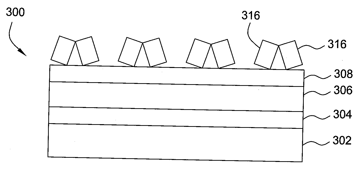
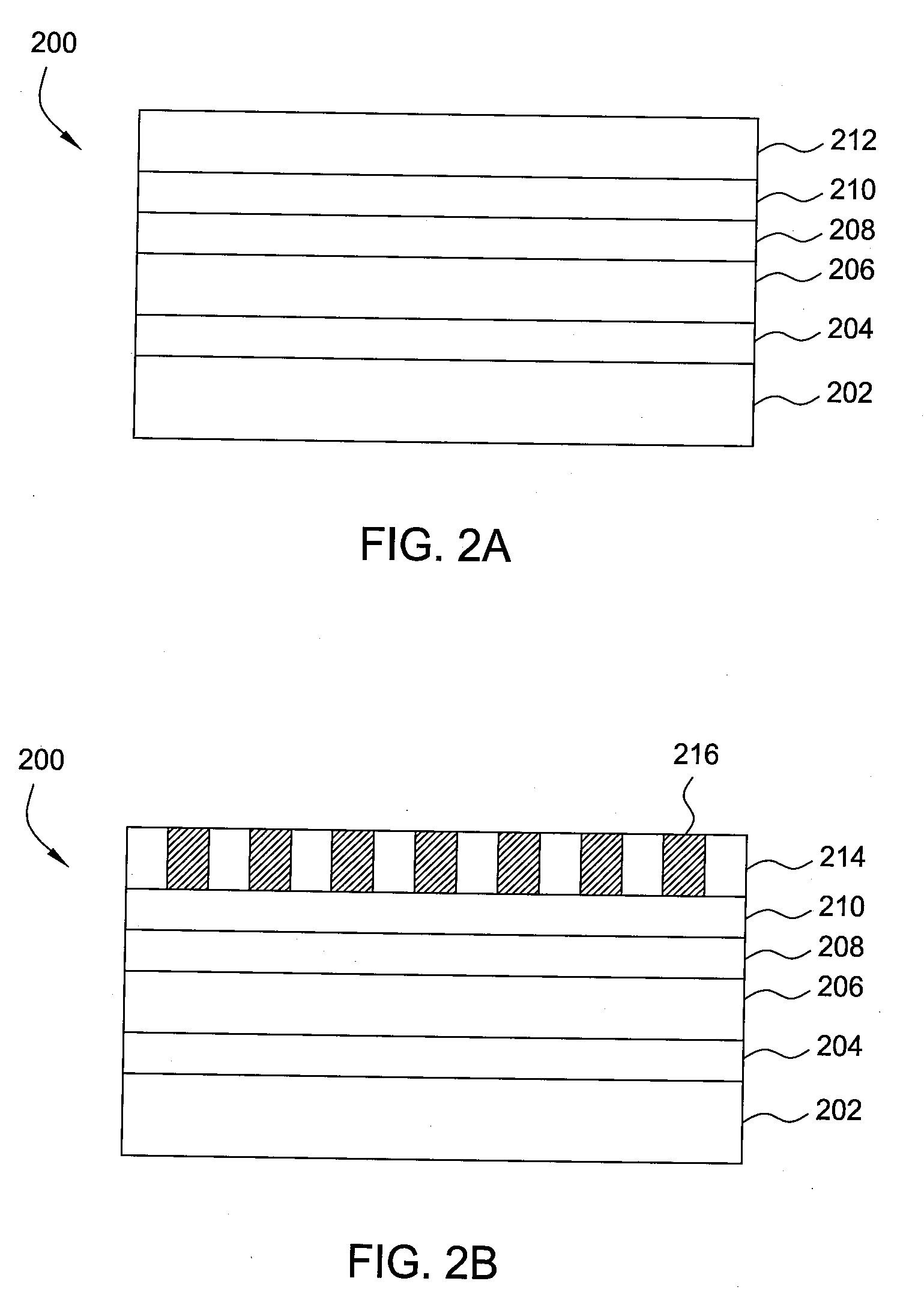
[0034]A hermetic oxide layer was deposited over a substrate having a layer stack consisting of a material layer, an amorphous carbon layer, and an ARC layer. The hermetic oxide layer was deposited at a temperature of 350 degrees Celsius and a pressure of 6 Torr. Process gases of 60 sccm silane and 9,900 sccm carbon dioxide were introduced into the chamber along with 10,000 sccm helium while the showerhead was biased with an RF frequency of 180 MHz and the substrate support was biased with an RF frequency of 180 MHz. The hermetic oxide layer was deposited to a thickness of 500 Angstroms. The hermetic oxide layer had tensile stress of 177 MPa when deposited. When the hermetic oxide layer was exposed to an atmosphere having 85 percent humidity at 85 degrees Celsius for 1 day, the oxide layer's stress changed to 176 MPa for a change in stress of 1 MPa. The hermetic oxide layer was stable and hence, the hermetic oxide layer did not fail under conditions designed to replicate dei...

Example

EXAMPLE 2

[0035]A hermetic oxide layer was deposited over a substrate having a layer stack consisting of a material layer, an amorphous carbon layer, and an ARC layer. The hermetic oxide layer was deposited at a temperature of 400 degrees Celsius and a pressure of 7 Torr. 50 sccm silane and 9,900 sccm carbon dioxide were introduced into the chamber along with 10,000 sccm helium while the showerhead was biased with an RF frequency of 140 MHz and the substrate support was biased with an RF frequency of 40 MHz. The hermetic oxide layer was deposited to a thickness of 2,741 Angstroms. The hermetic oxide layer had compressive stress of −214 MPa when deposited. When the hermetic oxide layer was exposed to an atmosphere having 85 percent humidity at 85 degrees Celsius for 1 day, the oxide layer's stress changed to −215 MPa for a change in stress of 1 MPa. The hermetic oxide layer was stable and hence, the hermetic oxide layer did not fail under conditions designed to replicate deionized wat...

Example

EXAMPLE 3

[0036]A hermetic oxide layer was deposited over a substrate having a layer stack consisting of a material layer, an amorphous carbon layer, and an ARC layer. The hermetic oxide layer was deposited at a temperature of 400 degrees Celsius and a pressure of 7 Torr. 50 sccm silane and 9,900 sccm carbon dioxide were introduced into the chamber along with 10,000 sccm helium while the showerhead was biased with an RF frequency of 140 MHz and the substrate support was biased with an RF frequency of 40 MHz. The hermetic oxide layer was deposited to a thickness of 2,827 Angstroms. The hermetic oxide layer had compressive stress of −200 MPa when deposited. When the hermetic oxide layer was exposed to an atmosphere having 85 percent humidity at 85 degrees Celsius for 1 day, the oxide layer's stress changed to −201 MPa for a change in stress of 1 MPa. The hermetic oxide layer was stable and hence, the hermetic oxide layer did not fail under conditions designed to replicate deionized wat...


PUM


Abstract

The present invention comprises a method of reducing photoresist mask collapse when the photoresist mask is dried after immersion development. As feature sizes continue to shrink, the capillary force of water used to rinse a photoresist mask approaches the point of being greater than adhesion force of the photoresist to the ARC. When the capillary force exceeds the adhesion force, the features of the mask may collapse because the water pulls adjacent features together as the water dries. By depositing a hermetic oxide layer over the ARC before depositing the photoresist, the adhesion force may exceed the capillary force and the features of the photoresist mask may not collapse.

Description

BACKGROUND OF THE INVENTION[0001]1. Field of the Invention[0002]Embodiments of the present invention generally relate to a method for preventing pattern collapse in immersion lithography.[0003]2. Description of the Related Art[0004]Integrated circuit geometries have dramatically decreased in size since such devices were first introduced several decades ago. Since then, integrated circuits have generally followed the two year / half-size rule (often called Moore's Law), which means that the number of devices on a chip doubles every two years. Today's fabrication facilities are routinely producing devices having 90 nm and even 65 nm feature sizes, and tomorrow's facilities soon will be producing devices having even smaller feature sizes such as 45 nm or smaller.[0005]As the feature sizes of integrated circuits decrease, so do the features of the photoresist mask used to pattern the features into the integrated circuit. Photoresist may be deposited, exposed, and then developed to create ...

Claims


Application Information

Patent Timeline
IPC IPC(8): G03F1/00
CPCG03F7/11G03F7/091G03F7/2041G03F7/40G03F7/70341H01L21/0273
Inventor KIM, EUI KYOONPADHI, DEENESHDAI, HUIXIONGNAIK, MEHULSEAMONS, MARTIN JAYKIM, BOK HOEN
Owner APPLIED MATERIALS INC
Why Eureka
Try Eureka