Deposition Method and Method for Manufacturing Light Emitting Device

a technology of light emitting devices and deposition methods, which is applied in the direction of electroluminescent light sources, vacuum evaporation coatings, coatings, etc., can solve the problems of long time required for processing the entire substrate and low productivity, and achieve high productivity, precise shape, and high precision

Inactive Publication Date: 2009-04-23
SEMICON ENERGY LAB CO LTD
View PDF18 Cites 47 Cited by
  • Summary
  • Abstract
  • Description
  • Claims
  • Application Information

AI Technical Summary

Benefits of technology

[0035]By application of the present invention, a film having a desired shape can be formed with high productivity. Specifically, a film having a precise shape ca

Problems solved by technology

However, in the methods shown in Reference 1 to 3, an only region to be transferred is irradiated with l

Method used


Image

  • Deposition Method and Method for Manufacturing Light Emitting Device
  • Deposition Method and Method for Manufacturing Light Emitting Device
  • Deposition Method and Method for Manufacturing Light Emitting Device

Examples


embodiment mode 1

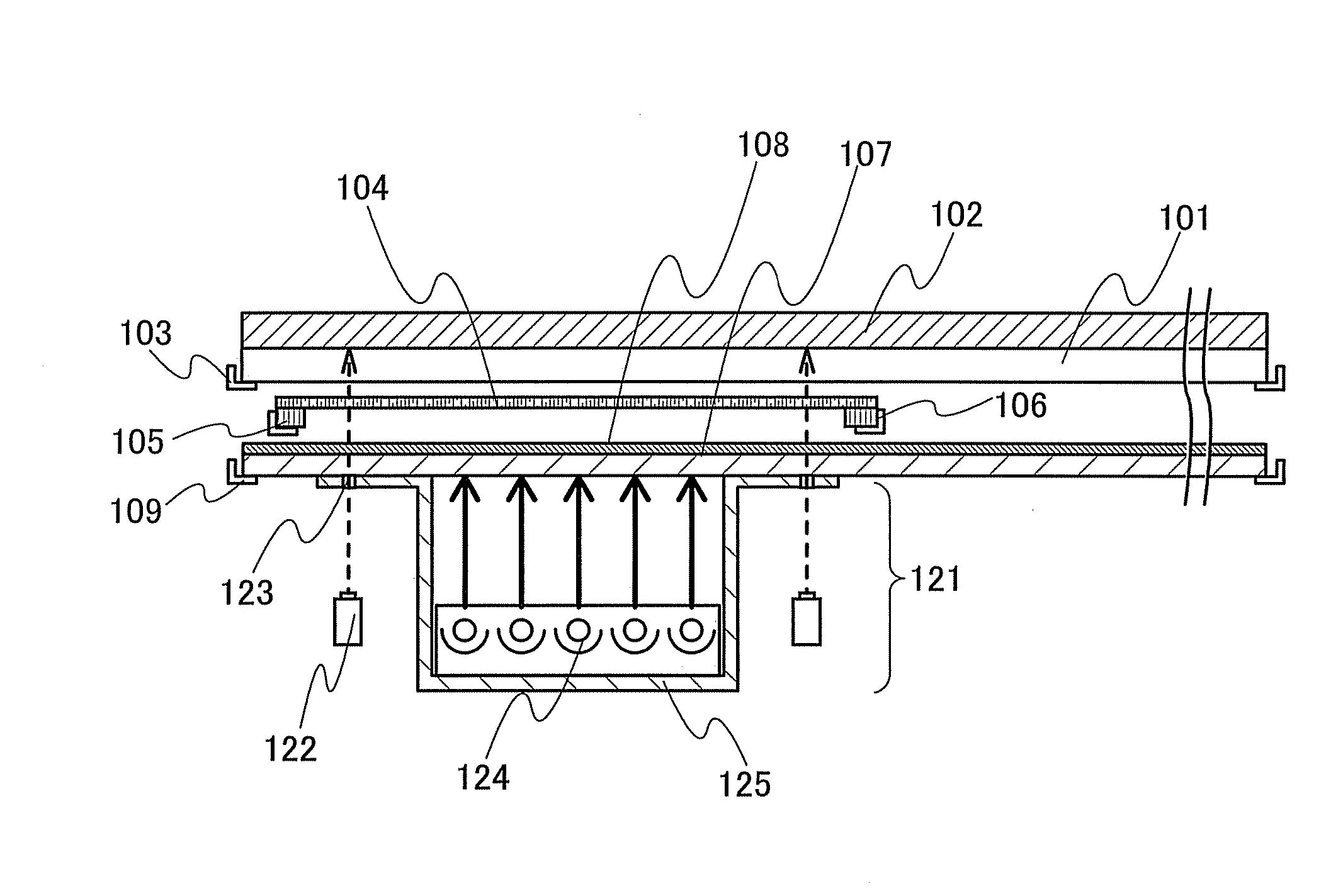
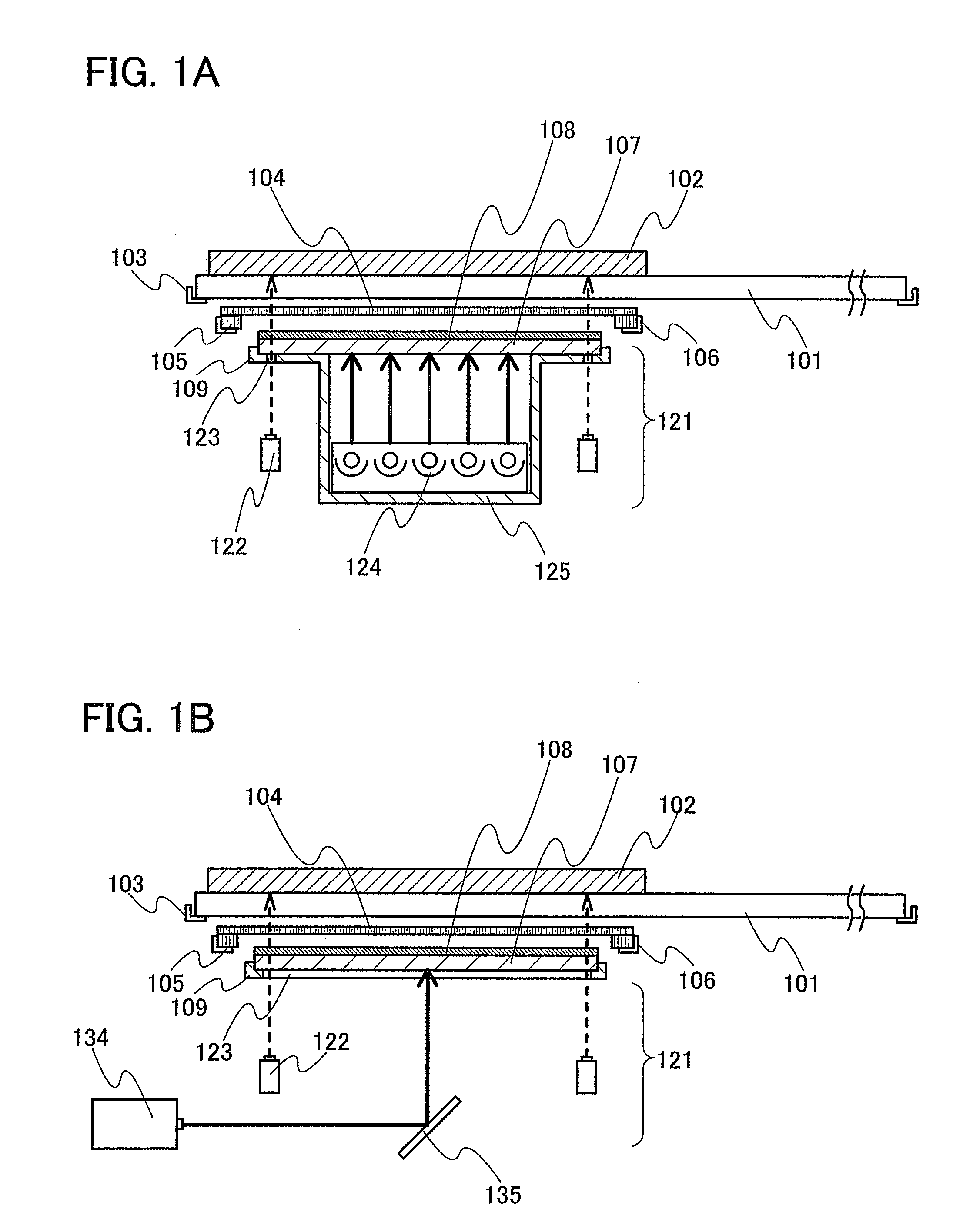
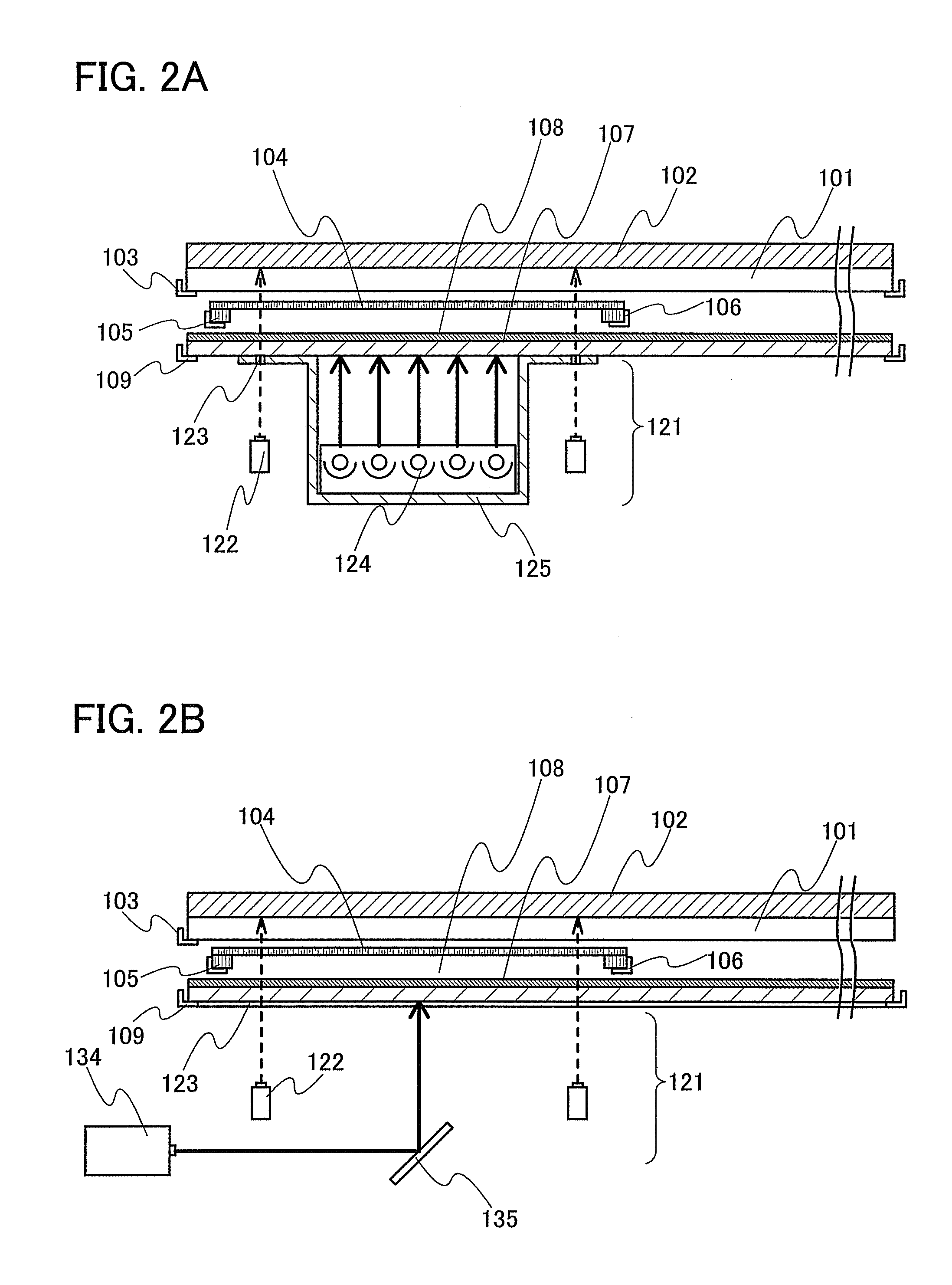
[0053]A deposition method and a method for manufacturing a light emitting device according to the present invention will be described with reference to FIGS. 1A and 1B, FIGS. 2A and 2B, FIG. 3, and FIGS. 4A and 4B.

[0054]In FIGS. 1A and 1B, a shadow mask 104 is placed between a deposition target substrate 101 and a supporting substrate 107 provided with an evaporation material 108. With an alignment means, the deposition target substrate 101 and the shadow mask are aligned with each other. Then, the evaporation material 108 provided for the supporting substrate 107 is heated by a deposition unit 121, and the vaporized evaporation material is deposited on the deposition target substrate 101 through an opening of the shadow mask 104.

[0055]The deposition target substrate 101 is held by a deposition target substrate holding means 103. The deposition target substrate holding means 103 may be part of a deposition target substrate transporting means. In the deposition target substrate 101, ...

embodiment mode 2

[0079]In this embodiment mode, a supporting substrate provided with an evaporation material, and a deposition method will be described in detail.

[0080]FIG. 4A shows an example of the supporting substrate provided with an evaporation material and the deposition target substrate. In FIG. 4A, a light absorption layer 201 is formed on a surface of a first substrate 200 that is a supporting substrate, which faces a second substrate that is a deposition target substrate. Further, an evaporation material is provided under the light absorption layer 201. In FIG. 4A, a material layer 202 containing the evaporation material is formed.

[0081]The first substrate 200 serves as a supporting substrate of the light absorption layer and the material layer, which transmits irradiated light for evaporating the evaporation material in a deposition process. Accordingly, the first substrate 200 is preferably a substrate having high light transmittance. Specifically, when lamp light or laser light is used ...

embodiment mode 3

[0113]In this embodiment mode, a method for manufacturing a full-color display device using a deposition method described in Embodiment Modes 1 and 2 is described.

[0114]Although FIGS. 4A and 4B show an example in which deposition is performed on each of the adjacent first electrode layers 207 in one deposition step, light emitting layers which emit light of different colors are formed in different regions in a plurality of deposition steps when a full-color display device is manufactured.

[0115]A manufacturing example of a light emitting device that is capable of full color display is described below. In this embodiment mode, an example of a light emitting device using light emitting layers which emit light of three colors is described.

[0116]Three supporting substrates provided with evaporation materials shown in FIG. 4A (evaporation donor substrates) are prepared. A plurality of layers each containing different evaporation material is formed over each of the irradiated substrates. S...


PUM

PropertyMeasurementUnit
Fractionaaaaaaaaaa
Thicknessaaaaaaaaaa
Thicknessaaaaaaaaaa

Abstract

An object is to provide a deposition method by which a film having a desired shape can be formed with high productivity. Further, a method for manufacturing a light emitting device by which a light emitting device having high definition can be manufactured with high productivity is provided. Specifically, even in the case of using a large-sized substrate, a method for manufacturing a light emitting device having high definition is provided. By using a deposition target substrate and a shadow mask having a smaller area than the deposition target substrate, the deposition target substrate and the shadow mask are aligned with each other, and an evaporation material is deposited on at least part of the deposition target substrate through a plurality of deposition steps. As an evaporation source, a light absorption layer and a supporting substrate having the evaporation material is preferably used.

Description

BACKGROUND OF THE INVENTION[0001]1. Field of the Invention[0002]The present invention relates to a deposition method and a method for manufacturing a light emitting device.[0003]2. Description of the Related Art[0004]An organic compound can have various structures in comparison with an inorganic compound, and it is possible to synthesize materials having various functions by appropriate molecular design. Because of these advantages, photo electronics and electronics using a functional organic material have been attracting attention in recent years.[0005]As examples of electronic devices using organic compounds as functional organic materials, there are solar cells, light emitting elements, organic transistors, and the like. These devices take advantage of electric properties and optical properties of the organic compound. Among them, in particular, light emitting elements have been making remarkable progress.[0006]It is said that, as for a light emitting mechanism of a light emittin...

Claims


Application Information

Patent Timeline
IPC IPC(8): H01L21/00B05D5/12
CPCC23C14/042C23C14/048C23C14/28H05B33/10H01L51/0013H01L51/56H01L27/3211H10K59/35H10K71/18H10K71/00
Inventor HIRAKATA, YOSHIHARUYAMAZAKI, SHUNPEI
Owner SEMICON ENERGY LAB CO LTD
Why Eureka
Try Eureka