Flexible Interposer for Stacking Semiconductor Chips and Connecting Same to Substrate

a technology of interposer and semiconductor chip, which is applied in the direction of solid-state devices, printed circuit aspects, basic electric elements, etc., can solve the problems of high failure rate, high cost, and limited number of connections of high-aspect ratio posts, and achieves reduced stress on contact joints, increased input/output, and reduced failure rate

Active Publication Date: 2009-05-14
TEXAS INSTR INC
View PDF12 Cites 47 Cited by
  • Summary
  • Abstract
  • Description
  • Claims
  • Application Information

AI Technical Summary

Benefits of technology

[0004]Applicant recognizes the need for a paradigm shift in chip assembly in order to accomplish simultaneously the benefit for a significantly higher number of inputs/outputs, for freedom of choosing chips of different sizes and rerouting needs, for higher reliability based on reduced stress on the contact joints and on low-k dielectrics in the chips, and on reduced package warpage, and for reduced pa

Problems solved by technology

They are difficult to form, expensive and have a high failure rate by cracks in the contact joints caused in temperature cycle testing and high

Method used


Image

  • Flexible Interposer for Stacking Semiconductor Chips and Connecting Same to Substrate
  • Flexible Interposer for Stacking Semiconductor Chips and Connecting Same to Substrate
  • Flexible Interposer for Stacking Semiconductor Chips and Connecting Same to Substrate

Examples


Embodiment Construction

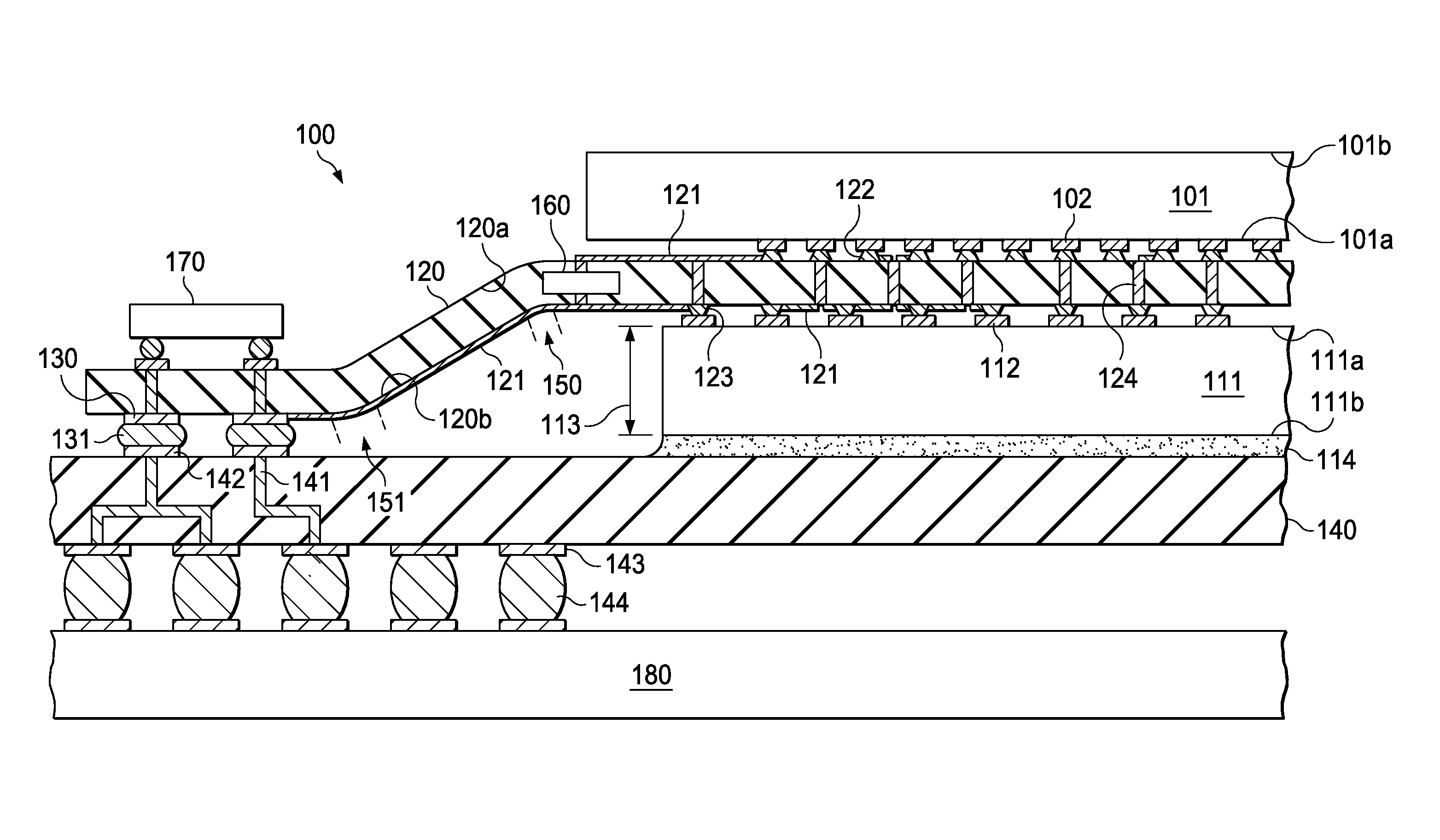
[0016]An embodiment of the invention is illustrated by the portion of a semiconductor device, generally designated 100, depicted in FIG. 1. Device 100 has a first semiconductor chip 101 and a second semiconductor chip 111. Chip 101 has a surface 101a with transistors or other integrated circuit components, and with terminals 102 in first locations; further, chip 101 has a surface 101b without transistors. For brevity, a surface with transistors is called herein an “active” surface, and a surface without transistors a “passive” surface. Both surfaces may, however, include metallic redistribution traces and pads for electrical connections. Chip 111 has a surface 111a with transistors or other integrated circuit components (“active” surface 111a), and with terminals 112 in second locations; further, chip 101 has a surface 111b without transistors (“passive” surface 111b), and a height or thickness 113.

[0017]It should be pointed out that in some embodiments, it may be advantageous for c...


PUM


Abstract

A semiconductor device with a first (101) and a second (111) semiconductor chip assembled on an insulating flexible interposer (120). The interposer, preferably about 25 to 50μm thick, has conductive traces (121), a central planar rectangular area and on each side of the rectangle a wing bent at an angle from the central plane. The central area has metal studs (122, 123) on the top and the bottom surface, which match the terminals of the chips, further conductive vias of a pitch center-to-center about 50 μm or less. The side wings have contact pads (130) with metallic connectors (131) on the bottom surface; the connectors may be solder balls, metal studs, or anisotropic conductive films. The second chip is adhesively attached to a substrate, whereby the interposer faces away from the substrate. The interposer side wings have a convex bending (150) downwardly along the second chip and a concave bending (151) over the substrate; the side wing connectors are attached to the matching substrate sites.

Description

FIELD OF THE INVENTION[0001]The present invention is related in general to the field of semiconductor devices and processes, and more specifically to low profile devices having a flexible interposer to integrate the chips vertically and to connect them to a substrate.DESCRIPTION OF RELATED ART[0002]Driven by the desire to reduce the board area needed to assemble a semiconductor device into electronic products such as hand-held telephones, today's semiconductor devices often use vertically stacked chips inside the packages. These chip stacks frequently include chips of significantly different sizes, assembled mostly by wire bonding techniques on interposers commonly made of rigid materials such as ceramics or fiber-enforced plastics such as FR-4 and others.[0003]After stacking the chips, the methodology to establish electrical connections from the stack to the substrate of the device or directly to the printed circuit board is most commonly a high-aspect ratio (height-to-width) metal...

Claims


Application Information

Patent Timeline
IPC IPC(8): H01L23/488H01L21/60
CPCH01L23/5384H01L2924/01087H01L23/5387H01L25/0657H01L25/162H01L2224/16H01L2224/73253H01L2225/06517H01L2225/06527H01L2225/06572H01L2924/01046H01L2924/01078H01L2924/01079H01L2924/14H01L2924/19041H01L2924/19042H01L2924/19043H01L2924/3025H05K1/028H05K1/141H05K1/147H05K1/189H05K2201/041H05K2201/10378H01L2924/01019H01L23/5386H01L2224/05568H01L2224/05573H01L2924/00014H01L2224/05599
Inventor WACHTLER, KURT PETER
Owner TEXAS INSTR INC
Why Eureka
Try Eureka