Semiconductor device having dual damascene structure

a technology of damascene structure and semiconductor device, which is applied in the direction of semiconductor device, semiconductor/solid-state device details, electrical apparatus, etc., can solve the problems of easy layer separation, easy interlayer insulation film, and large improvement space, so as to reduce the capacitance between wirings and improve the assembling yield

Active Publication Date: 2009-05-14
RENESAS ELECTRONICS CORP
View PDF8 Cites 19 Cited by
  • Summary
  • Abstract
  • Description
  • Claims
  • Application Information

AI Technical Summary

Benefits of technology

[0017]According to an exemplary aspect of the present invention, therefore, it is possible to provide a semiconductor device capable of reducing the capacitance between wirings in each wiring layer having a narrow wiring

Problems solved by technology

However, any of the above-described techniques leaves much room for improvement on the following points.
However, in case of the power wiring layer having a wide wiring pi

Method used


Image

  • Semiconductor device having dual damascene structure
  • Semiconductor device having dual damascene structure
  • Semiconductor device having dual damascene structure

Examples


Embodiment Construction

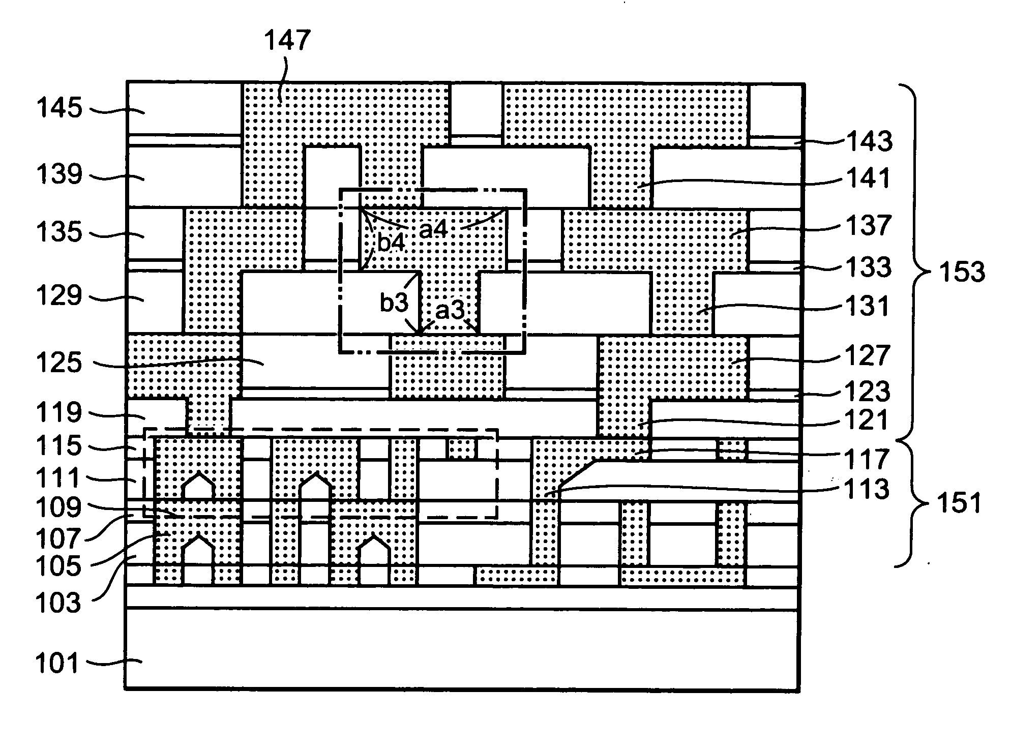
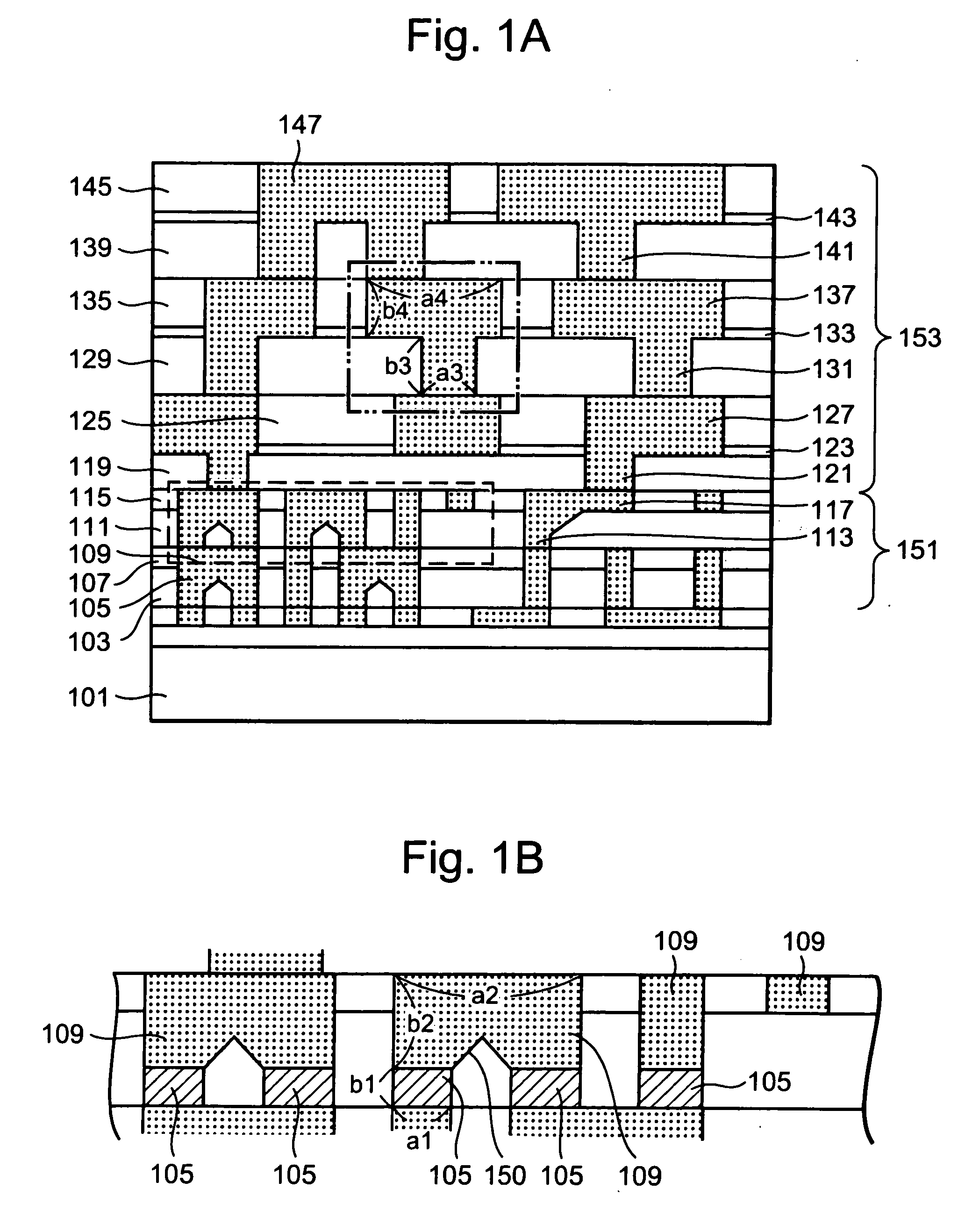
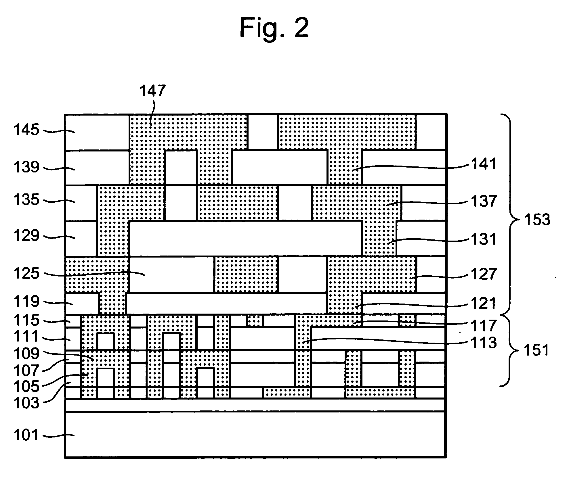
[0027]FIG. 1A is an exemplary cross sectional view of a semiconductor device in a embodiment. FIG. 1B is an enlarged view of the portion surrounded in a dot line of FIG. 1A. In the exemplary embodiment, the semiconductor device includes multilayer wirings of a dual damascene structure. The multilayer wirings of the dual damascene structure mean a structure in which many via layers and many wiring layers that include vias and wirings of a dual damascene structure respectively are stacked. Furthermore, the semiconductor device includes a local wiring layer 151 (first wiring layer) formed on a semiconductor substrate 101 and a power wiring layer 153 (second wiring layer) formed on the local wiring layer 151.

[0028]The local wiring layer 151 includes an insulation film 103 (first insulation film), plural first vias 105 provided in the insulation film 103, an insulation film 107 (second insulation film) provided on the insulation film 103, and a first wiring 109 provided on the first vias...


PUM


Abstract

The semiconductor device includes multilayer wirings of a dual damascene structure. The multilayer wirings include a first wiring layer formed on a semiconductor substrate and a second wiring layer formed on the first wiring layer. The first wiring layer includes a first insulation film, plural first vias provided in the first insulation film, a second insulation film provided on the first insulation film, and a first wiring provided on the first vias and connected to those first vias in the second insulation film. The second wiring layer includes a third insulation film, plural second vias provided in the third insulation film, an adhesive layer provided on the third insulation film, a fourth insulation film provided on the adhesive layer, and a second wiring provided on the second vias and connected to those second vias in the fourth insulation film. In the first wiring layer, the aspect ratio L of a wiring having the minimum wiring width and the via aspect ratio V are in a relationship of L≧V and in the second wiring layer, the aspect ratio L of a wiring having the minimum wiring width and the via aspect ratio V is in a relationship of L<V.

Description

BACKGROUND OF THE INVENTION[0001]1. Field of the Invention[0002]The present invention relates to a semiconductor device having a multilayer wiring structure formed by a dual damascene method.[0003]2. Description of Related Art[0004]FIG. 2 shows a technique related to a semiconductor device having a multilayer wiring structure as a related art. FIG. 2 shows a cross sectional view of a semiconductor device having a local wiring layer 151 and a power wiring layer 153. Elements such as transistors, not shown, are formed on a semiconductor substrate 101 and on the surface are provided the local wiring layer 151 and the power wiring layer 153. Each of the local wiring layer 151 and the power wiring layer 153 has a dual damascene wiring structure, in which no stopper is provided at the phase boundary between a via layer and a wiring layer (hereinafter, this structure is referred to as the stopper-less structure). The via layer means a layer that includes an interlayer insulation film provi...

Claims


Application Information

Patent Timeline
IPC IPC(8): H01L21/768H01L23/522
CPCH01L21/76804H01L21/76808H01L23/5283H01L23/5286H01L2924/0002H01L23/5329H01L2924/00
Inventor TAKEWAKI, TOSHIYUKI
Owner RENESAS ELECTRONICS CORP
Why Eureka
Try Eureka