Semiconductor integrated circuit

a technology of integrated circuits and semiconductors, applied in the direction of resistors, electrical devices, arrangements responsive to excess voltage, etc., can solve the problems of difficult to reduce the output capacitance cb>total, difficult to make the capacitance cb>2, and difficulty in properly triggering the thyristor, etc., to achieve low output capacitance and reduce the resistance value of the path

Active Publication Date: 2009-05-14
RENESAS ELECTRONICS CORP
View PDF13 Cites 25 Cited by
  • Summary
  • Abstract
  • Description
  • Claims
  • Application Information

AI Technical Summary

Benefits of technology

[0021]According to the present invention, it is possible to provide a semiconductor integrated circuit which can simultaneously achieve reduction in the resistance value of the path to which the output signal is outputted and reliability in triggering of the ESD protection device while having a low output capacitance.

Problems solved by technology

A problem caused by using the thyristor as the ESD protection device is difficulty in properly triggering the thyristor, in particular, in triggering the thyristor with a low voltage.
This problem is serious, especially, if a gate of the NMOS transistor N1 of the last stage output driver 116 is in the floating state when the ESD surge is applied to the output pad 112.
Since it is difficult to reduce a junction area between the N well 132 and the P well 133, it is difficult to make the capacitance C2 smaller, which means that it is difficult to reduce the output capacitance Ctotal.
Increase in an output capacitance of the output pad 112 is disadvantageous in outputting an output signal at high speed.
However, the semiconductor integrated circuit 300 in FIG. 5 has a problem that decrease in the resistance value of a path to which an output signal is outputted and reliability in triggering of the thyristor 114 cannot be achieved at a time.
As a result, even when the ESD surge is applied, the thyristor 114 is hard to operate.

Method used


Image

  • Semiconductor integrated circuit
  • Semiconductor integrated circuit
  • Semiconductor integrated circuit

Examples


first embodiment

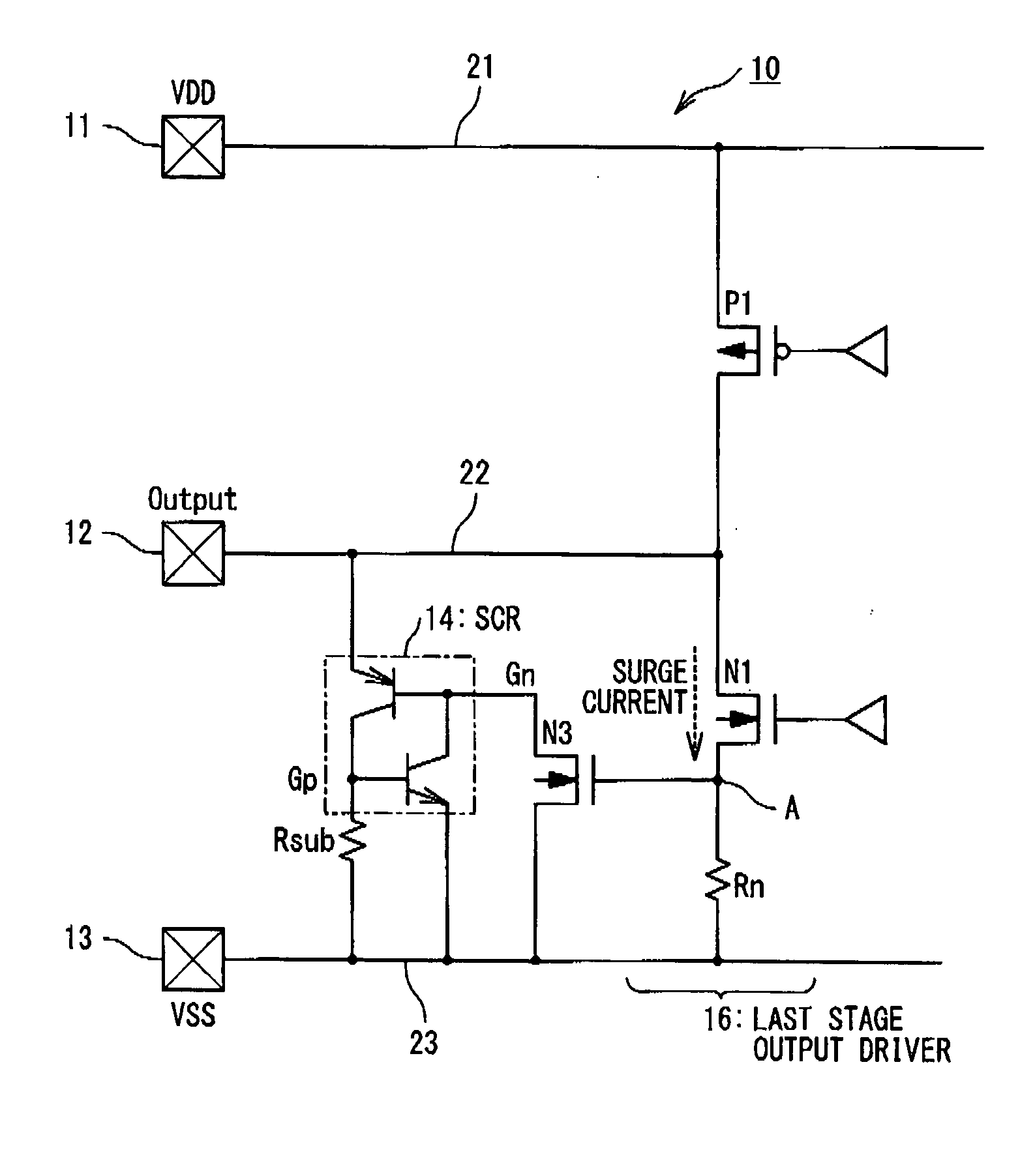
[0041]FIG. 6A is a circuit diagram showing a configuration of a semiconductor integrated circuit 10 according to a first embodiment of the present invention. The semiconductor integrated circuit 10 has a VDD pad 11 connected to a power supply line 21, an output pad 12 connected to an output signal line 22, a VSS pad 13 connected to a ground line 23 and a thyristor 14. The VDD pad 11 serves as a power supply terminal to which a power supply voltage is supplied, and the VSS pad 13 serves as a ground terminal to be grounded. The output pad 12 is used to output an output signal to an external unit. The thyristor 14 has a function of discharging ESD surge to the ground line 23 when the ESD surge is applied to the output pad 12.

[0042]A last stage output driver 16 of an internal circuit is connected to the output signal line 22. The last stage output driver 16 has a PMOS transistor P1 connected between the power supply line 21 and the output signal line 22 and an NMOS transistor N1 connect...

second embodiment

[0052]FIG. 9 is a circuit diagram showing the configuration of a semiconductor integrated circuit 10A according to a second embodiment of the present invention. The semiconductor integrated circuit 10A of the second embodiment has the configuration for protecting the PMOS transistor P1 of the last stage output driver 16 from the electrostatic breakdown. In detail, a resistance element Rp is connected between the power supply line 21 and a node B and the PMOS transistor P1 is connected between the node B and the output signal line 22. The resistance element Rp is used to detect a current flowing through the PMOS transistor P1 as a protection target device. The PMOS transistor P3 used as a trigger device is connected to the P gate Gp of the thyristor 14. The PMOS transistor P3 is connected to the P gate Gp of the thyristor 14 at its drain, is connected to the node B at its source and is connected to the power supply line 21 at its gate. A power clamp 17 is connected between the power ...

third embodiment

[0056]FIG. 10 is a circuit diagram showing the configuration of a semiconductor integrated circuit 10B according to a third embodiment of the present invention. The semiconductor integrated circuit 10B in the third embodiment has the configuration of a combination of the semiconductor integrated circuits 10 and 10A in the first and second embodiments, for protecting both of the NMOS transistor N1 and the PMOS transistor P1 against electrostatic breakdown. In detail, the resistance element Rn is connected between the ground line 23 and the node A and the NMOS transistor N1 is connected between the node A and the output signal line 22. The gate of the NMOS transistor N3 used as the trigger device is connected to the node A. The NMOS transistor N3 is connected to the N gate Gn of the thyristor 14 at its drain, and is connected to the ground line 23 at its source. Furthermore, the resistance element Rp is connected between the power supply line 21 and the node B and the PMOS transistor ...


PUM


Abstract

A semiconductor integrated circuit includes: an output pad from which an output signal is outputted; an output signal line connected with the output pad; a first pad configured to function as a ground terminal or a power supply terminal; a first wiring connected with the first pad; an output driver connected with the output pad and configured to generate the output signal; an ESD protection device connected with the output signal line and having a function to discharge surge applied to the output pad; and a first trigger MOS transistor used as a trigger device. The output driver includes: a first protection target device connected between the output signal line and the first interconnection; and a first resistance element connected between the first protection target device and the first interconnection. The first trigger MOS transistor configured to detect a voltage generated in the first resistance element by a gate of the first trigger MOS transistor and to allow the ESD protection device operate in response to the detected voltage.

Description

INCORPORATION BY REFERENCE [0001]This application claims a priority on convention based on Japanese Patent Application No. 2007-293233. The Disclosure thereof is incorporated herein by reference.BACKGROUND OF THE INVENTION [0002]1. Field of the Invention[0003]The present invention relates to a semiconductor integrated circuit, and more particularly, to a semiconductor integrated circuit provided with an ESD (electrostatic discharge) protection device for preventing breakdown of an internal circuit due to application of an ESD surge.[0004]2. Description of Related Art[0005]A semiconductor integrated circuit is generally provided with an ESD protection device for protecting an internal circuit from ESD surge applied to an input / output pad. The ESD protection device discharges the ESD surge applied to the input / output pad to a power supply line or a ground line, thereby protecting the internal circuit.[0006]A thyristor is a typical ESD protection device. Since the thyristor has high di...

Claims


Application Information

Patent Timeline
Patent Type & Authority Applications(United States)
IPC IPC(8): H02H9/00
CPCH01L27/0262
Inventor OKUSHIMA, MOTOTSUGU
Owner RENESAS ELECTRONICS CORP
Why Eureka
Try Eureka