Current driver device

a current driver and driver technology, applied in the direction of speech analysis, semiconductor devices, instruments, etc., can solve the problems of low process cost of amorphous silicon, low yield, reliability, etc., and achieve the effect of high speed

Inactive Publication Date: 2009-05-28
LAPIS SEMICON CO LTD
View PDF5 Cites 11 Cited by
  • Summary
  • Abstract
  • Description
  • Claims
  • Application Information

AI Technical Summary

Benefits of technology

[0013]That is, there is provided a second current source for compensating for charging by a parasitic capacitance even when the parasitic capacitance exists in each data line (circuit to be driven). Accordingly, the charging by the parasitic capacitance is canceled out, and a pixel circuit or the like of a display device, which is connected to each data line, can be charged at high speed. Incidentally, the second current source operates as a negative capacitance with respect to the parasitic capacitance.

Problems solved by technology

The amorphous silicon is low in process cost, but has a problem of reliability depending on a threshold voltage shift based on the time of use.
Due to it, a problem occurs in that yields are reduced.
A problem however arises in that due to the parasitic capacitance of each data line, a write time interval becomes long due to the current in a driver based on the current-driven system.
In particular, a problem arises in that the time is taken under the current of a low level.
A problem however arises in that the parasitic capacitance exists in each pixel electric circuit to which a line (data line) for the data signal is connected, and the writing (charging) of data into the holding capacitor become slow due to the parasitic capacitance.
A problem however arises in that the charging time increases as a current value becomes low, and data cannot be written within the allowable time as the case may be.
There is however a demerit that the comparing capacitance is large and the area of a driver increases.
Such methods are also quite complex.

Method used


Image

  • Current driver device
  • Current driver device
  • Current driver device

Examples


first preferred embodiment

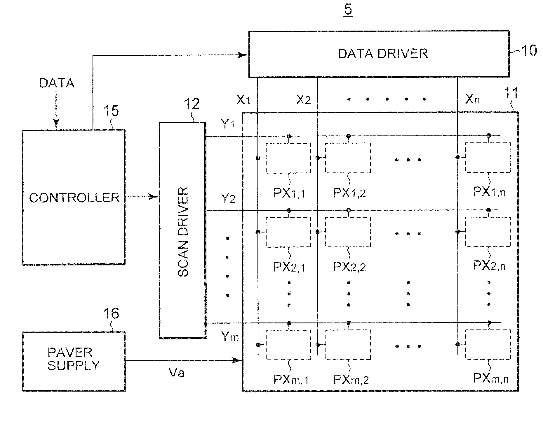
[0024]A driver device (data driver) according to the present invention will be explained below. FIG. 1 typically shows a display device 5 as one example of a device in which a data driver 10 illustrative of a first preferred embodiment of the present invention is used.

[0025]The display device 5 is provided with the data driver 10, a display panel 11, a scan driver 12, a controller 15 and a light-emitting element driving power source PS (hereinafter also called simply “power source PS”) 16.

[0026]The display panel 11 is of an active matrix type display panel comprised of pixels of m rows and n columns (m×n: m and n being integers greater than or equal to 1). The display panel 11 has a plurality of scan lines Y1 through Ym (where Yi: i=1 through m) respectively disposed in parallel, a plurality of data lines X1 through Xn (Xj: j=1 through n) respectively orthogonal to the scan lines, and a plurality of pixels PX1,1 through PXm,n. The pixels PX1,1 through PXm,n are respectively disposed...

second preferred embodiment

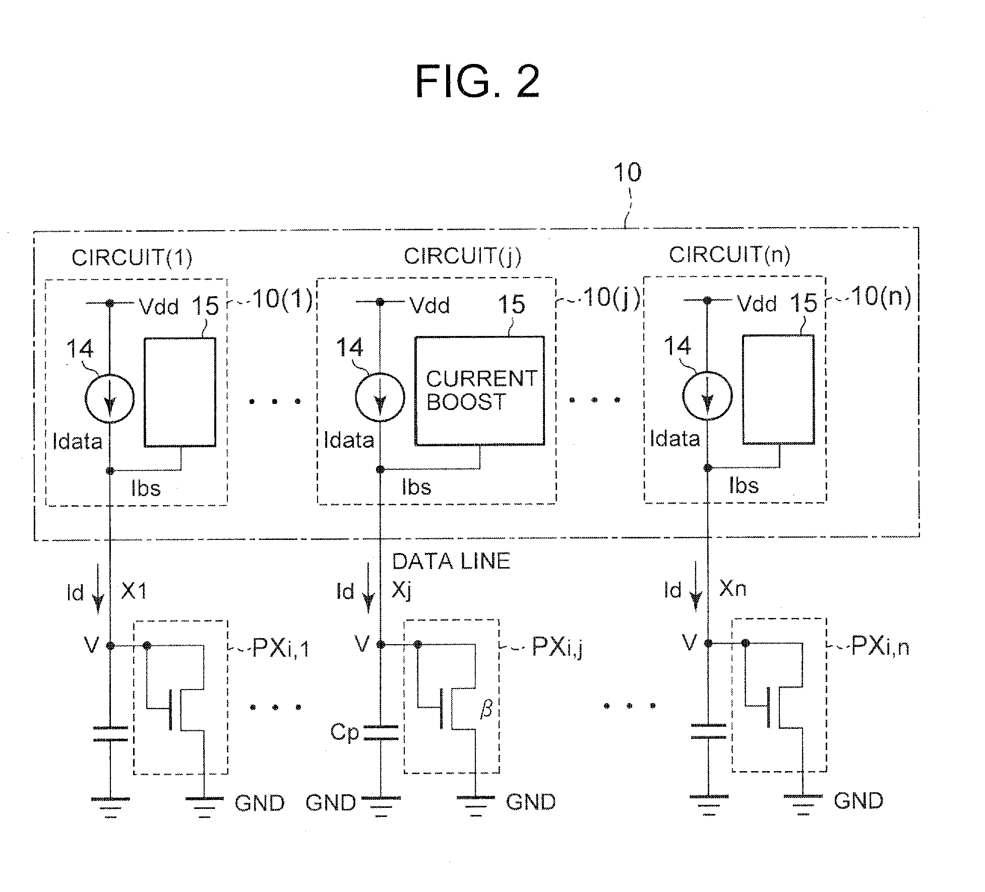
[0047]FIG. 8 is a circuit diagram showing one example of a concrete circuit of a current boost circuit 15 illustrative of a second preferred embodiment of the present invention.

[0048]In the V-I conversion circuit 18 employed in the first preferred embodiment, the resistor R3 connected in series to the transistor 26 operated as the variable current source is substituted with a transistor M3, thereby making it possible to control a boost current value with a high degree of accuracy. That is, a gate voltage Vg of the transistor M3 connected in series to the transistor 26 is changed on an analog basis thereby to enable its resistance value to vary effectively instead of the resistor R3. It is however necessary to operate the transistor M3 in a linear region.

[0049]Incidentally, there is provided a constant current sink circuit 31 which causes a bias current produced in the current boost circuit 15 to flow into a ground (GND) line.

[0050]Alternatively, a plurality of transistors different ...


PUM


Abstract

The present invention provides a current-driven driver device capable of current writing at high speed even when a parasitic capacitance exists in a circuit to be driven. Each of current driver circuits includes a first current source for supplying a data current of a current value corresponding to a data signal, and a second current source including a differentiation circuit generating a differential value of a voltage applied to each data line and for supplying a boost current of a current value corresponding to the differential value to the data line.

Description

BACKGROUND OF THE INVENTION [0001]The present invention relates to a driver circuit, and particularly to a driver device for driving a display device such as an active matrix display including light-emitting elements such as an LED (light-emitting diode) and the like.[0002]A display device using an organic light emitting diode (OLED) has been in the limelight as a promising next-generation display. A passive matrix organic light emitting diode (PM-OLED) display has been industrialized and applied in many fields in recent years. There has however been a demand for high performance inclusive of a main display of a cellular phone, etc. In order to find widespread application to various products, there is a need to apply an active matrix organic light emitting diode (AM-OLED) display thereto.[0003]AM-OLEDs are divided according to materials that constitute transistors, i.e., amorphous silicon, low-temperature polysilicon, micro crystal silicon, high-temperature polysilicon, etc. The amo...

Claims


Application Information

Patent Timeline
Patent Type & Authority Applications(United States)
IPC IPC(8): G10L19/02
CPCG09G3/3241G09G2320/029G09G2310/0248G09G3/3283H01L2027/11879H01L2924/13069
Inventor FUKUZAKO, SHINICHIHATTORI
Owner LAPIS SEMICON CO LTD
Why Eureka
Try Eureka