Semiconductor device

a technology of semiconductor devices and semiconductors, applied in semiconductor devices, instruments, computing, etc., can solve the problems of reducing the yield of products and adversely affecting the characteristics of elements, and achieve the effects of reducing damage to elements such as transistors, reducing stress, and increasing yield and reliability of semiconductor devices

Inactive Publication Date: 2009-06-04
SEMICON ENERGY LAB CO LTD
View PDF9 Cites 39 Cited by
  • Summary
  • Abstract
  • Description
  • Claims
  • Application Information

AI Technical Summary

Benefits of technology

[0006]In view of the above problems, an object of the present invention is to provide a semiconductor device in which damages of an element such as a transistor are reduced even when external force such as bending is externally applied to the semiconductor device.
[0007]An aspect of the present invention is a semiconductor device in which a reinforcement film is provided to suppress generation of stress in an element such as a transistor, even when external force such as bending is applied to the semiconductor device, in manufacturing the semiconductor device or in use of the completed semiconductor device. The reinforcement film is provided so that, in the thickness direction of a semiconductor device, a neutral plane (a plane which does not expand or contract) in which distortion of stress such as tensile stress or compressive stress is not caused due to deformation such as bending can be located at a preferred position for the semiconductor device.
[0010]As a feature of the first island-like reinforcement film and the second island-like reinforcement film, the first island-like reinforcement film and the second island-like reinforcement film are formed using a material higher Young's modulus than the semiconductor film. Specifically, the first island-like reinforcement film and the second island-like reinforcement film are formed using silicon nitride, silicon nitride oxide, metal oxide, metal nitride or the like. By forming the first island-like reinforcement film and the second island-like reinforcement film using a material higher Young's modulus than the semiconductor film, the mechanical strength of the semiconductor film can be increased and damages to the semiconductor film can be reduced without changing the properties of the semiconductor film.
[0012]By provision of a reinforcement film in an element such as a transistor constituting a part of a semiconductor device, it is possible to suppress generation of stress in an element such as a transistor, even when external force such as bending is applied to the semiconductor device, in manufacturing the semiconductor device or in use of the completed semiconductor device. Accordingly, damages to an element such as a transistor can be reduced and yield and reliability of a semiconductor device can be increased.

Problems solved by technology

However, when external force such as bending is externally applied to a semiconductor device including an integrated circuit provided with an element such as a transistor over a flexible substrate, stress caused in the semiconductor device might damage the element such as a transistor which is included in the semiconductor device and adversely affect characteristics of the element.
Further, in the manufacturing process of the semiconductor device, the element such as a transistor is stressed and therefore the element might be damaged, which results in reducing the yield of products.

Method used


Image

  • Semiconductor device
  • Semiconductor device
  • Semiconductor device

Examples


embodiment mode 1

[0036]In Embodiment Mode 1, an example of a semiconductor device will be described with reference to drawings.

[0037]In this embodiment mode, a reinforcement film is provided to suppress generation of stress in an element such as a transistor, even when external force such as bending is applied to the semiconductor device. In this embodiment mode, as an example, a case is described where reinforcement films formed from a material having an elastic modulus higher than Young's modulus of the semiconductor film, above and below the semiconductor film constituting a part of the transistor.

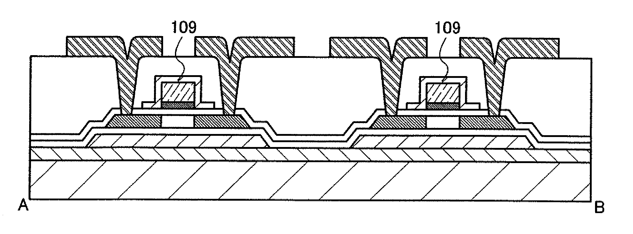
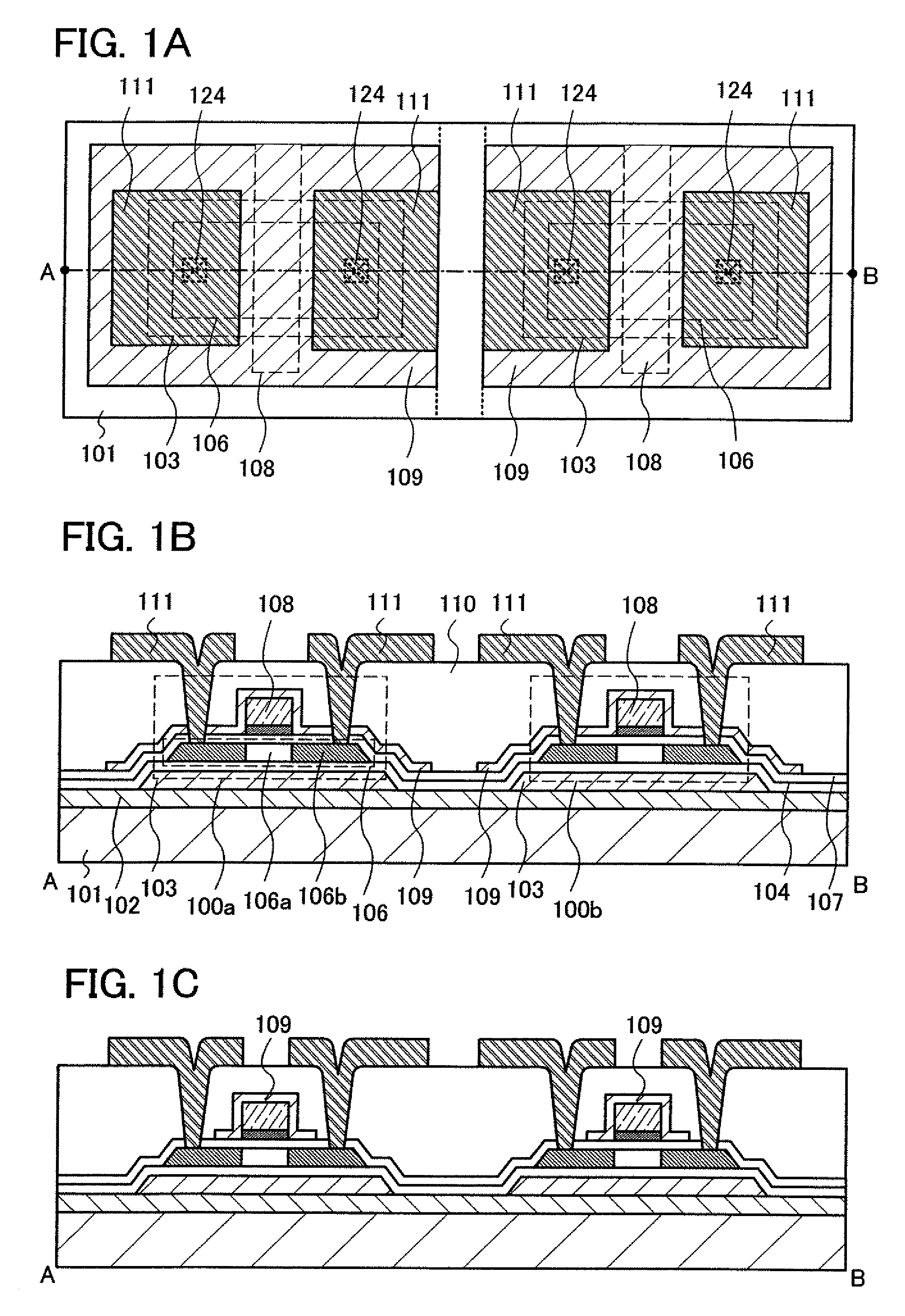
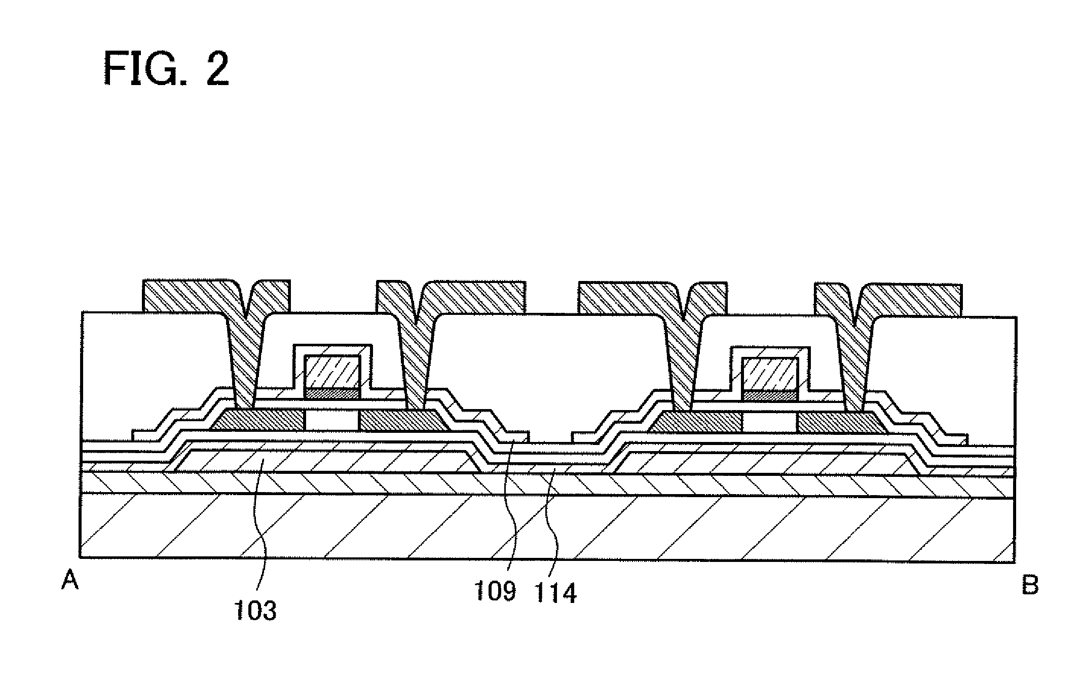
[0038]FIGS. 1A to 1C illustrate an example of the semiconductor device described in this embodiment mode. Note that FIG. 1A illustrates a top plan view, and FIG. 1B illustrates a cross-sectional view taken along a line A-B in FIG. 1A.

[0039]The semiconductor device illustrated in FIG. 1B has thin film transistors 100a and 100b, which at least include a semiconductor film 106, a gate insulating film 107, ...

embodiment mode 2

[0056]In Embodiment Mode 2, an example of a method for manufacturing the semiconductor device described in Embodiment Mode 1 is described with reference to drawings. Note that in this embodiment mode, the process is described in which after an element such as a thin film transistor is formed over a supporting substrate, the element is separated from the supporting substrate to be transferred to another substrate. In this specification, “transfer” means that an element formed over a substrate is moved to another substrate.

[0057]First, a release layer 121 is formed over a surface of a substrate 120, and an insulating film 102 serving as a buffer layer, and a reinforcement film are formed. Note that the release layer 121, the insulating film 102 and the reinforcement film can be formed successively. Then, the reinforcement film is subjected to selective etching using a resist mask formed by a photolithography method, so that an island-like reinforcement film 103 is formed (FIG. 4A).

[00...

embodiment mode 3

[0095]In this embodiment mode, the case where, in a thin film transistor of the semiconductor device described in Embodiment Mode 1 or 2, an insulating film is formed to be in contact with a side surface of the first conductive film functioning as a gate electrode and an LDD region is formed below the insulating film is described with reference to drawings.

[0096]FIGS. 7A and 7B show an example of the semiconductor device described in this embodiment mode. Note that FIG. 7A illustrates a top plan view and FIG. 7B illustrates a cross-sectional view taken along a line A-B in FIG. 7A.

[0097]The semiconductor device described in this embodiment mode includes the thin film transistors 100a and 100b, and insulating films 130 are provided to be in contact with a side surface of the first conductive films 108 functioning as gate electrodes, which are included in the thin film transistors 100a and 100b (see FIGS. 7A and 7B). The insulating films 130 are also referred to as side walls, and a st...


PUM


Abstract

A semiconductor device in which damages to an element such as a transistor are reduced even when external force such as bending is applied and stress is generated in the semiconductor device. The semiconductor device includes a first island-like reinforcement film over a substrate having flexibility; a semiconductor film including a channel formation region and an impurity region over the first island-like reinforcement film; a first conductive film over the channel formation region with a gate insulating film interposed therebetween; a second island-like reinforcement film covering the first conductive film and the gate insulating film.

Description

BACKGROUND OF THE INVENTION[0001]1. Field of the Invention[0002]The present invention relates to a semiconductor device, in particular, a semiconductor device in which damages of an element such as a transistor provided in the semiconductor device are reduced even when an external force is applied.[0003]2. Description of the Related Art[0004]In recent years, a technique for providing an integrated circuit including a transistor or the like over a flexible substrate such as a plastic substrate has attracted attention. A semiconductor device formed by providing an integrated circuit over a flexible substrate can be reduced in weight, cost, or the like as compared to the case of using a substrate such as a semiconductor substrate or a glass substrate. Since a flexible semiconductor device can be bent for example, it is expected to be applied to various fields and places (Reference 1: Japanese Patent No. 4015002, Reference 2: Japanese Published Patent Application No. 2006-232449, and Re...

Claims


Application Information

Patent Timeline
Patent Type & Authority Applications(United States)
IPC IPC(8): G06K19/077H01L29/00H01L29/786
CPCH01L27/1218H01L29/78603
Inventor YAMAZAKI, SHUNPEIGOTO, YUUGOMURAKAWA, TSUTOMU
Owner SEMICON ENERGY LAB CO LTD
Why Eureka
Try Eureka