Active material devices with containment layer

a technology of active materials and containment layers, which is applied in the direction of bulk negative resistance effect devices, semiconductor devices, electrical equipment, etc., can solve the problems of volatilization and volumetric loss of active materials, and achieve the effect of preventing or inhibiting

Active Publication Date: 2009-06-04
OVONYX MEMORY TECH LLC
View PDF4 Cites 23 Cited by
  • Summary
  • Abstract
  • Description
  • Claims
  • Application Information

AI Technical Summary

Benefits of technology

[0011]The instant invention provides electronic devices having a contained active material. The active material may be a memory material, switching material, chalcogenide material, pnictide material, or phase-change material. In the device, the active material is in electrical communication with a lower electrode and an upper electrode. The upper electrode is capped with a containment layer to prevent or inhibit volatilization of the active material during high temperature steps in the fabrication process or during operation when high temperatures are produced locally within the active material during the programming process. The containment layer further protects the active material from chemical contamination from the processing environment during fabrication or the ambient environment during operation. The upper electrode may be deposited conformally or non-conformally over the active material. The upper electrode may be a single conductive layer or a stack of two or more conductive layers which may differ in resistivity. A diffusion barrier layer and / or breakdown layer may optionally be included between the active material and either or both of the upper and lower electrodes. The containment layer may be deposited conformally or non-conformally over the upper electrode.

Problems solved by technology

During fabrication or operation, the device is often exposed to high temperatures that promote volatilization and volumetric loss of the active material.

Method used


Image

  • Active material devices with containment layer
  • Active material devices with containment layer
  • Active material devices with containment layer

Examples


example 1

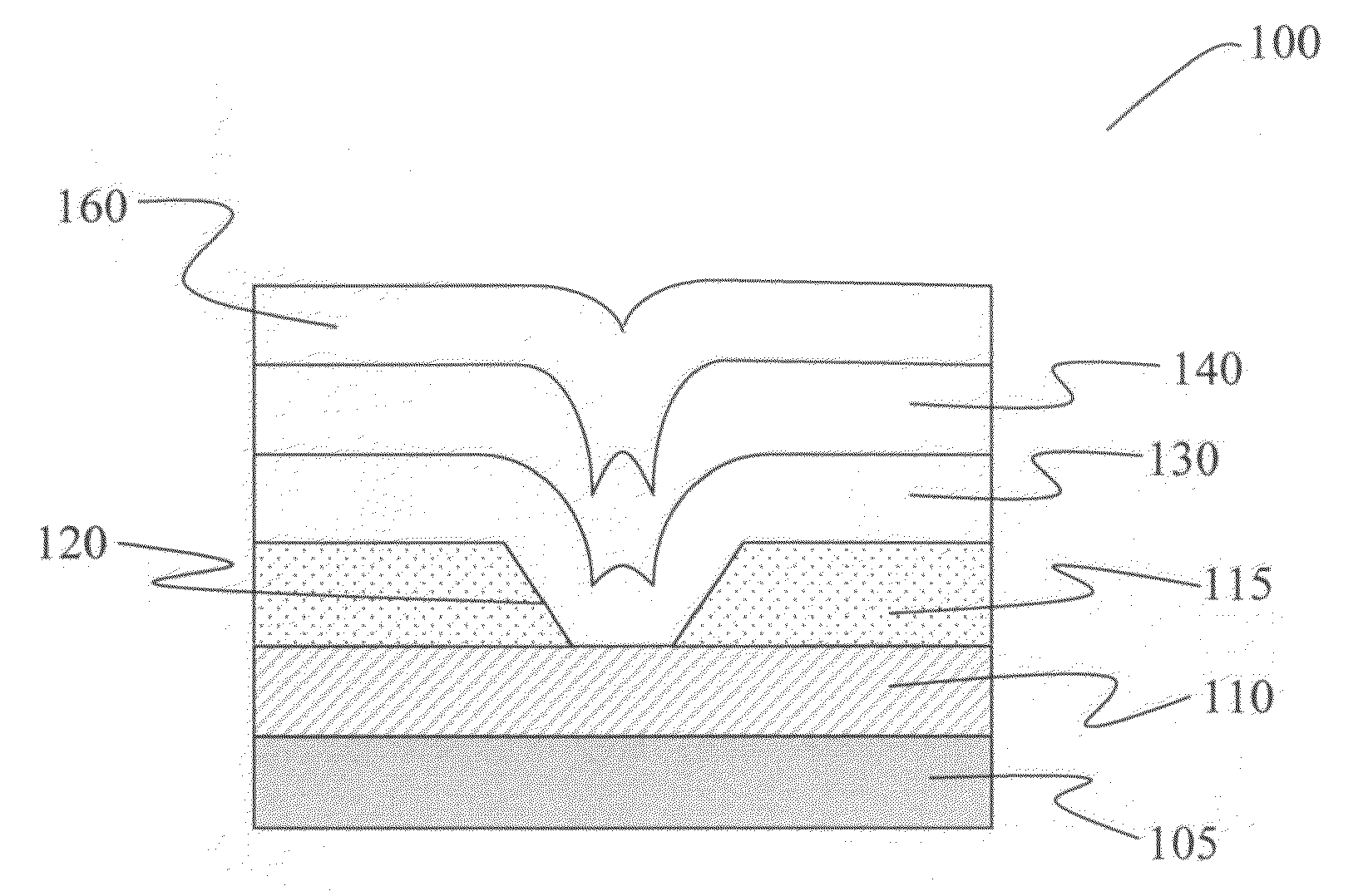
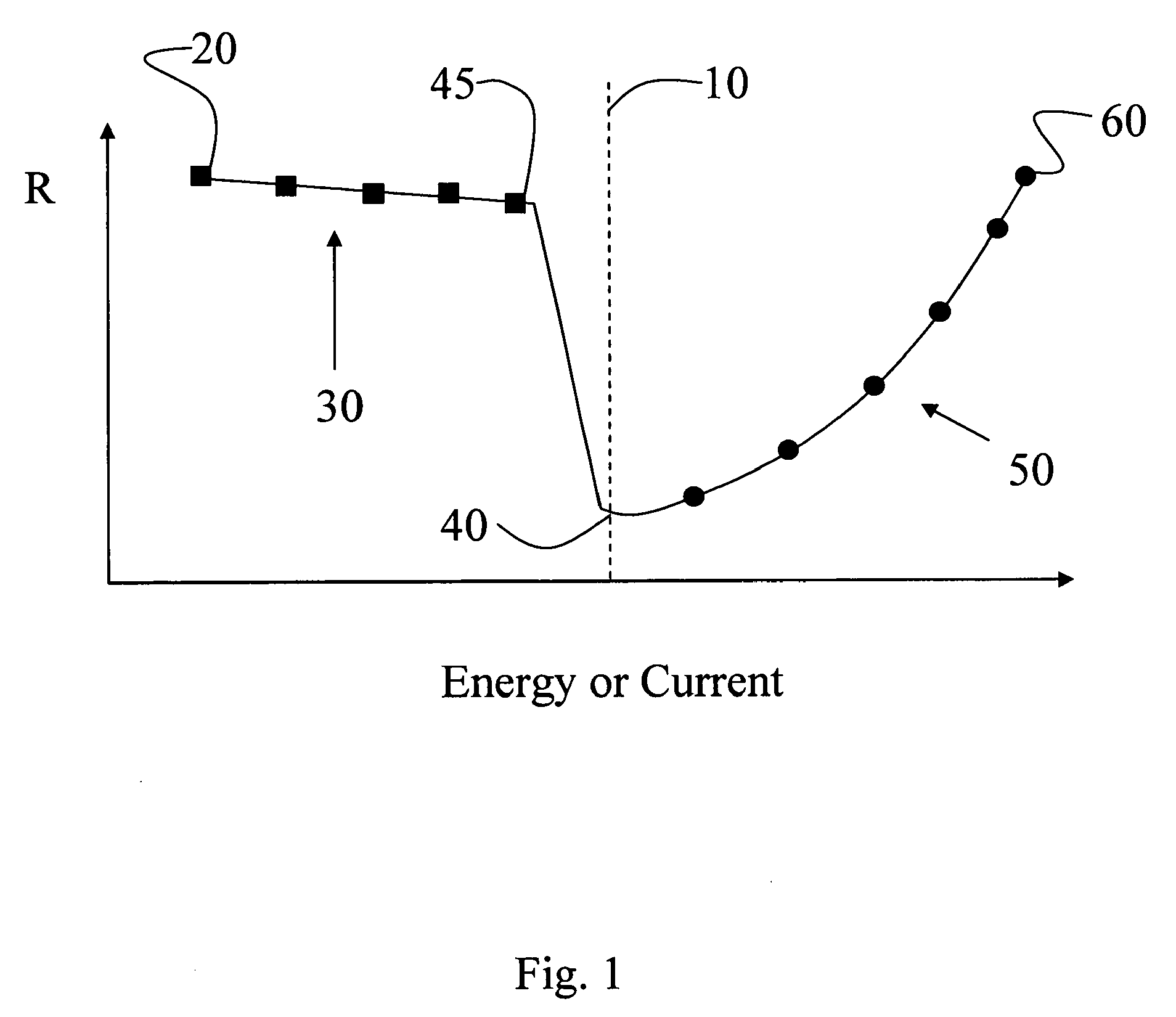
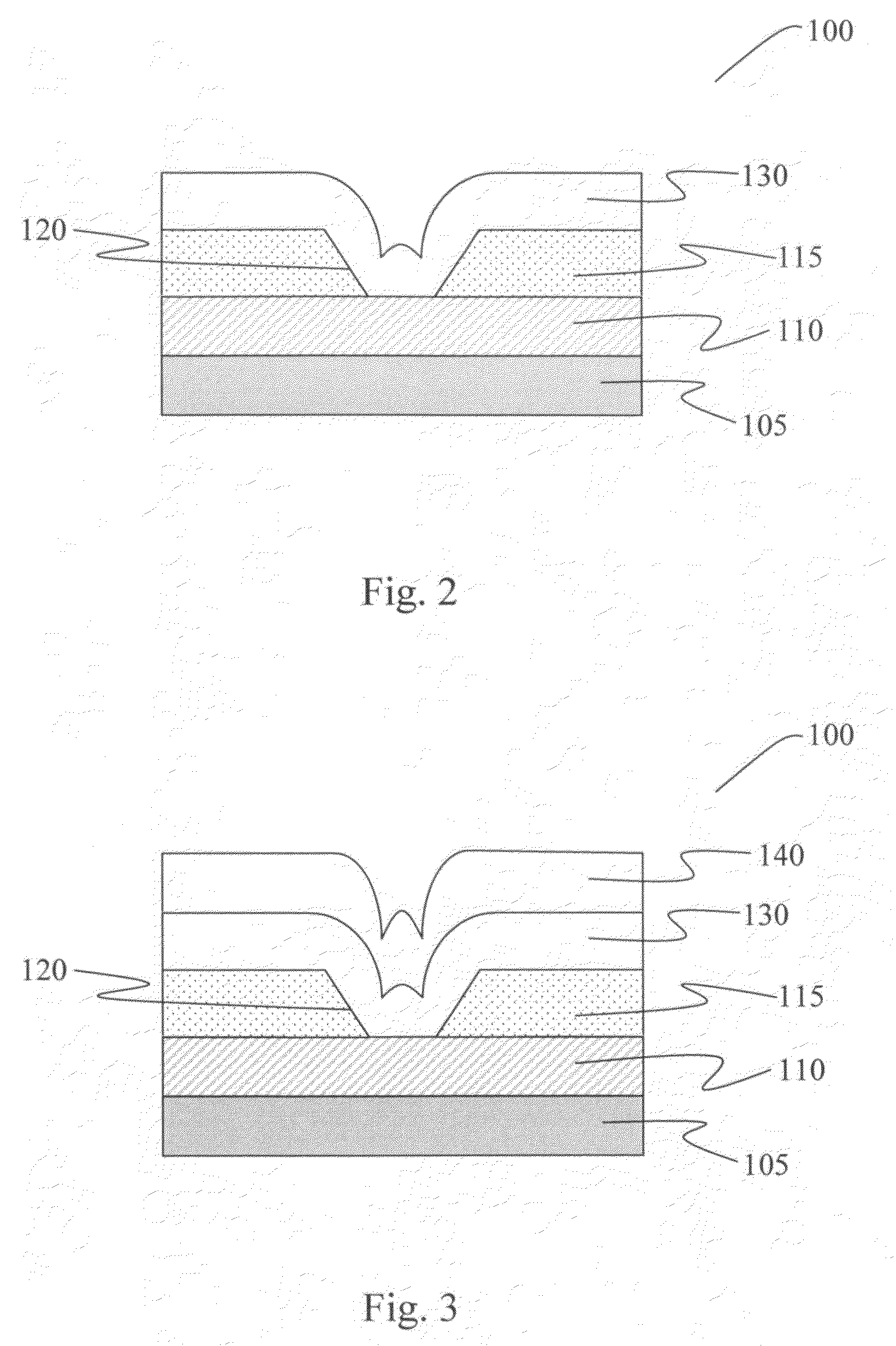
[0068]In this example, electronic devices having a pore cell design are compared and it is demonstrated that inclusion of a containment layer provides a significant extension of the cycle life of the device. A cross-sectional micrograph of the device used in this example is shown in FIG. 7. The device 200 includes substrate 205 that includes an oxide surface layer, a TiAIN lower electrode 210 (˜650 Å thick), insulator 215 (˜375 Å thick), active layer 220 that comprises a chalcogenide phase-change material (Ge2Sb2Te5) (˜750 Å thick), and a Ti / TiN upper electrode 225 (˜20 Å of Ti in contact with active layer 220 and ˜600 Å of TiN formed thereover). Substrate 205, lower electrode 210, and insulator 215 formed a base wafer upon which active layer 220 and upper electrode 225 were deposited using a low temperature sputtering process. Electronic device 200 has a pore cell design analogous to that shown in FIG. 3. Note that active layer 220 occupies an opening in insulator 215 (near center ...


PUM


Abstract

An active material electronic device is described with a containment layer. The device includes an active chalcogenide, pnictide, or phase-change material in electrical communication with an upper and lower electrode. The device includes a containment layer formed over the active material that prevents escape of volatilized matter from the active material when the device is exposed to high temperatures during fabrication or operation. The containment layer further prevents chemical contamination of the active material by protecting it from reactive species in the processing or ambient environment. The containment layer and intermediate layers formed between the active material and containment layer are formed at temperatures sufficiently low to prevent volatilization of the active material. Once the containment layer is formed, the device may be subjected to high temperature or chemically aggressive environments without impairing the compositional or structural integrity of the active material. Inclusion of the containment layer is shown to extend the cycle life of the device by over two orders of magnitude.

Description

FIELD OF INVENTION[0001]This invention relates to electronic devices having volatile active materials susceptible to evaporation during processing or operation at elevated temperatures. More particularly, this invention relates to methods of making electronic devices that include protective steps designed to prevent evaporation of active materials during fabrication or operation. Most particularly, this invention relates to methods of making chalcogenide or phase-change memory or switching devices that include low temperature deposition of a containment layer to confine a volatile active material during subsequent high temperature processing or operation.BACKGROUND OF THE INVENTION[0002]Chalcogenide materials are an emerging class of commercial electronic materials that exhibit switching, memory, logic, and processing functionality. The basic principles of chalcogenide materials were developed by S. R. Ovshinsky in the 1960's and much effort by him and others around the world since ...

Claims


Application Information

Patent Timeline
Patent Type & Authority Applications(United States)
IPC IPC(8): H01L45/00
CPCH01L45/06H01L45/12H01L45/1233H01L45/141H01L45/1641H01L45/144H01L45/148H01L45/1625H01L45/143H10N70/231H10N70/801H10N70/826H10N70/8825H10N70/882H10N70/8828H10N70/884H10N70/026H10N70/041H10N70/068
Inventor SANDOVAL, REGINO
Owner OVONYX MEMORY TECH LLC
Why Eureka
Try Eureka