Substrate-free light emitting diode chip

Inactive Publication Date: 2009-06-04
GOLDENEYE
View PDF7 Cites 128 Cited by
  • Summary
  • Abstract
  • Description
  • Claims
  • Application Information

AI Technical Summary

Benefits of technology

[0012]A substrate-free or free-standing LED chip of this invention is an LED chip that does not include a growth substrate or transfer substrate as an element of the LED chip. The growth substrate is defined as the substrate onto which the multilayer semiconductor structure is epitaxially grown. For LED chips of this invention, the growth substrate is removed after the multilayer semiconductor structure is fabricat

Problems solved by technology

However, none of these additional surfaces, submounts, heat sin

Method used


Image

  • Substrate-free light emitting diode chip
  • Substrate-free light emitting diode chip
  • Substrate-free light emitting diode chip

Examples


Embodiment Construction

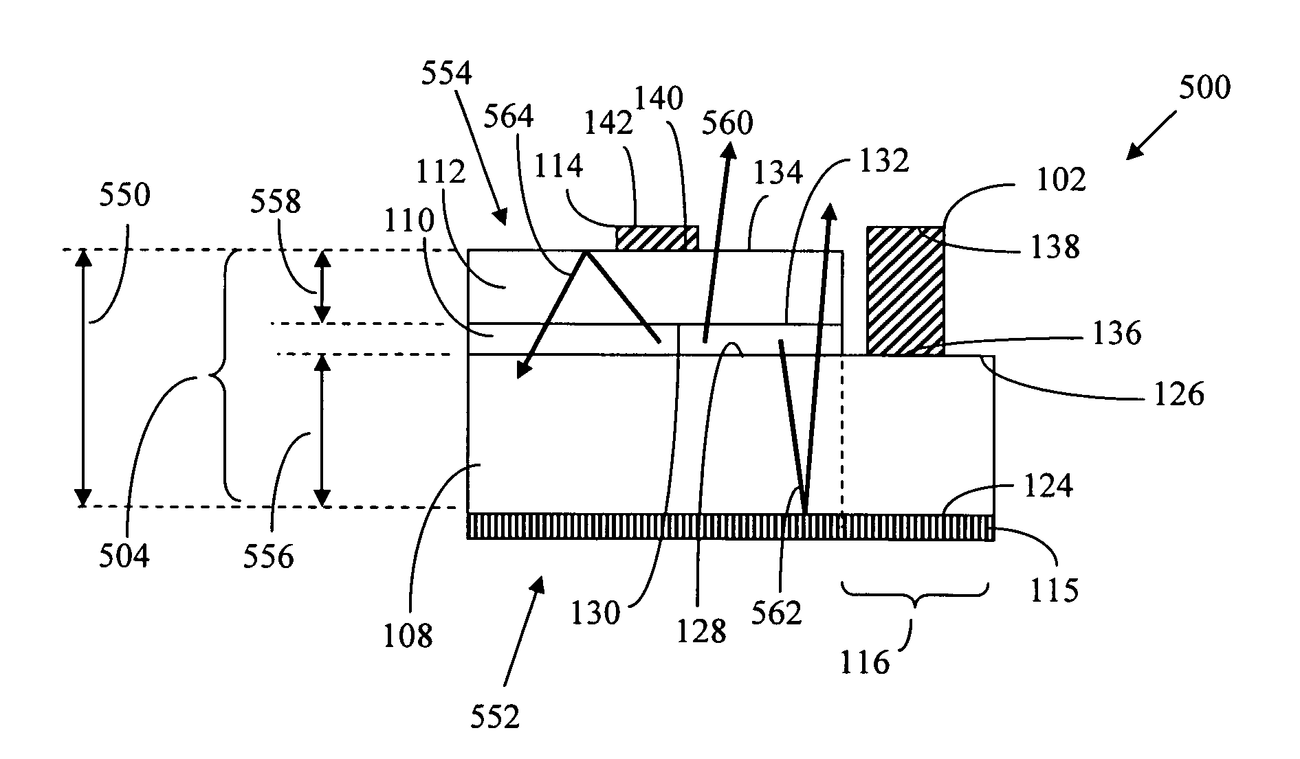
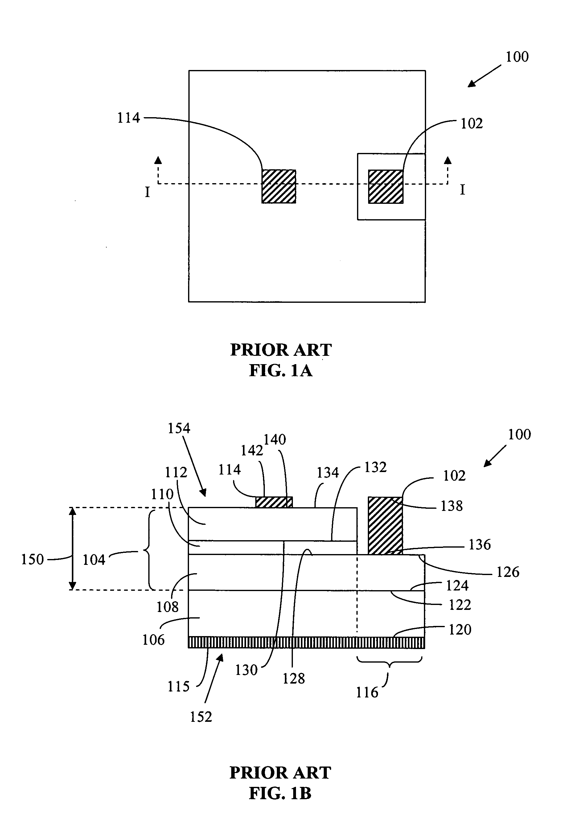
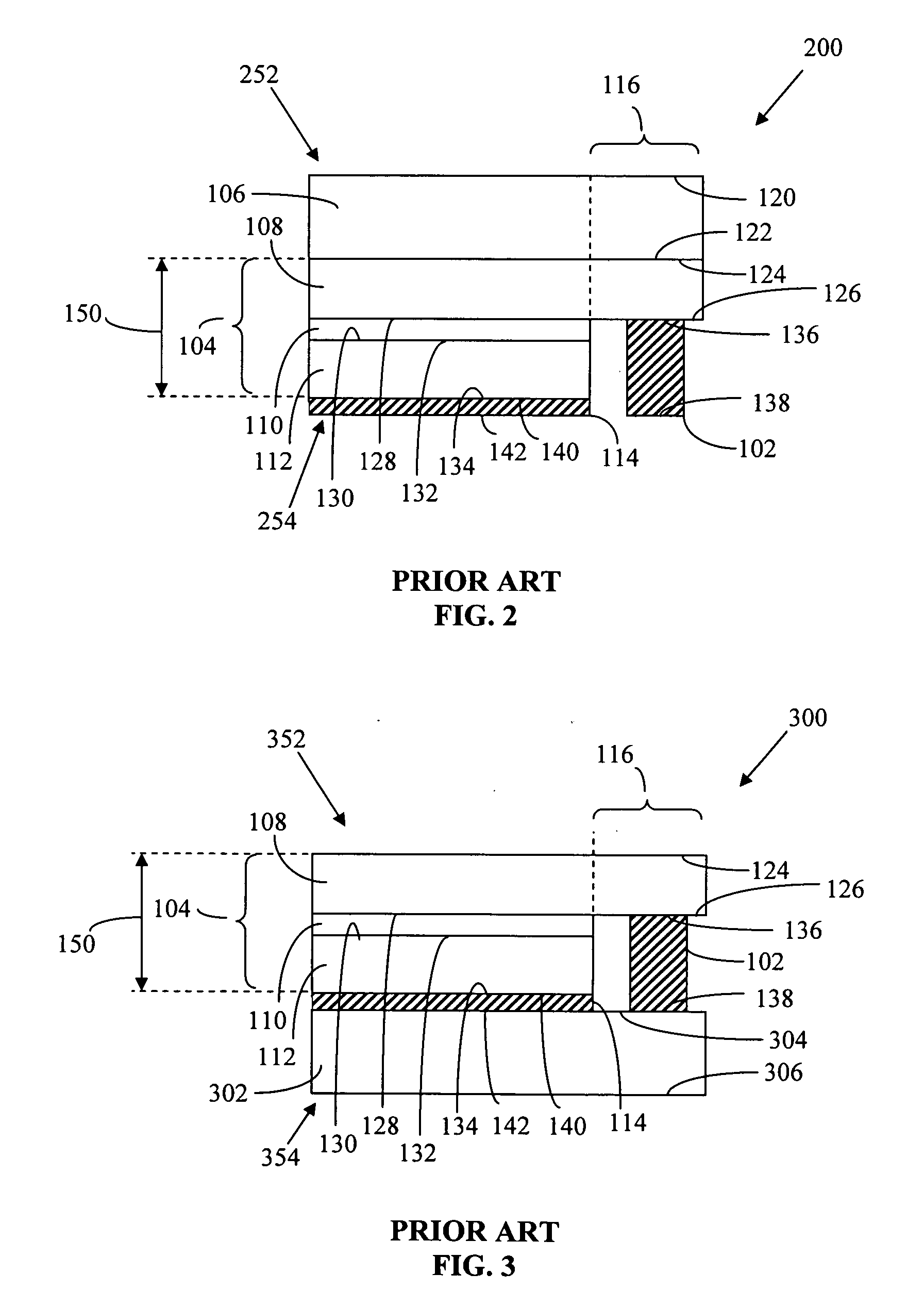
[0036]The preferred embodiments of the present invention will be better understood by those skilled in the art by reference to the above listed figures. The preferred embodiments of this invention illustrated in the figures are not intended to be exhaustive or to limit the invention to the precise form disclosed. The figures are chosen to describe or to best explain the principles of the invention and its applicable and practical use to thereby enable others skilled in the art to best utilize the invention. For ease of understanding, the thicknesses of the layers in the semiconductor structures in the figures are not drawn to scale.

[0037]Light emitting diodes can be fabricated by epitaxially growing multiple layers of semiconductors on a growth substrate. Inorganic light-emitting diodes can be fabricated from gallium nitride (GaN) based semiconductor materials containing, for example, gallium nitride (GaN), aluminum nitride (AlN), aluminum gallium nitride (AlGaN), indium nitride (In...


PUM


Abstract

A light emitting diode (LED) chip has a multilayer semiconductor structure that is at least 10 microns thick and does not require an attached growth substrate or transfer substrate for structural rigidity or support. The multilayer semiconductor structure includes a first doped layer, a second doped layer and an active region interposed between the first doped layer and the second doped layer. Optionally, the multilayer semiconductor structure includes an undoped layer. At least one of the layers of the multilayer semiconductor structure is at least 5 microns thick and is preferably deposited by hydride vapor phase epitaxy.

Description

REFERENCE TO PRIOR APPLICATION[0001]This application claims the benefit of U.S. Provisional Patent Application Ser. No. 61 / 005,258, which was filed on Dec. 3, 2007, and which is herein incorporated by reference.TECHNICAL FIELD[0002]The present invention is a thick light emitting diode chip. The chip is substrate-free or free-standing and requires no growth substrate or transfer substrate for structural support.BACKGROUND OF THE INVENTION[0003]Conventional light emitting diodes (LEDs) are fabricated by epitaxially growing multiple layers of semiconductors on a growth substrate. Inorganic light-emitting diodes can be fabricated from GaN-based semiconductor materials containing, for example, gallium nitride (GaN), aluminum nitride (AlN), aluminum gallium nitride (AlGaN), indium nitride (InN), indium gallium nitride (InGaN) and aluminum indium gallium nitride (AlInGaN). Other appropriate materials for LEDs include, for example, aluminum gallium indium phosphide (AlGaInP), gallium arseni...

Claims


Application Information

Patent Timeline
IPC IPC(8): H01L33/00H01L33/32H01L33/42H01L33/50H01L33/62
CPCH01L25/0753H01L33/32H01L33/42H01L33/505H01L33/508H01L33/62H01L2924/0002H01L33/648H01L2933/0083H01L2924/00
Inventor ZIMMERMAN, SCOTT M.BEESON, KARL W.LIVESAY, WILLIAM R.ROSS, RICHARD L.
Owner GOLDENEYE
Why Eureka
Try Eureka