Solid-state imaging device and camera

a solid-state imaging and camera technology, applied in the field of solid-state imaging devices and cameras, can solve the problems of reducing the gate size of the pixel transistor included in pixels, affecting the image quality of the image, so as to suppress the leak current from the photoelectric conversion element to the floating diffusion region, the effect of increasing the ease of generation

Inactive Publication Date: 2009-06-04
SONY CORP
View PDF9 Cites 82 Cited by
  • Summary
  • Abstract
  • Description
  • Claims
  • Application Information

AI Technical Summary

Benefits of technology

[0017]In the pixel included in the solid-state imaging device according to an embodiment of the invention, the channel width of the transfer gate of the transfer transistor on the side of the floating diffusion region is formed to be larger than on the side of the photoelectric conversion element. As a result, even when the pixel size is miniaturized, the potential of a channel region becomes deeper on the side of floating diffusion region than on the side of photoelectric conversion element when the transfer gate is turned on during a readout period, and the electrical field can be generated with more ease in the direction of charge transfer. In addition, when the transfer transistor is turned off, the leak current from the

Problems solved by technology

With regard to CMOS image sensor, the gate size of the pixel transistors included in pixels decreases with the decrease in pixel size, and it has become more difficult to maintain the characteristics of the pixel transistors.
That is, the leak current is generated more easily from a photodiode (PD) to a floating diffusion (FD) region when the transfer gate is turned off, while a potential barrier has become difficult to be sufficiently lowered when the transfer gate is turned on for the readout period because of weak channel modulation by the transfer gate.
However, there exist trade-offs between the size of transfer gate

Method used


Image

  • Solid-state imaging device and camera
  • Solid-state imaging device and camera
  • Solid-state imaging device and camera

Examples


Embodiment Construction

[0029]The present invention will be described hereinbelow on a variety of embodiments by referring to the accompanying drawings. It is not intended to be exhaustive or to limit the invention to those disclosed in the embodiments and illustrated in the drawings.

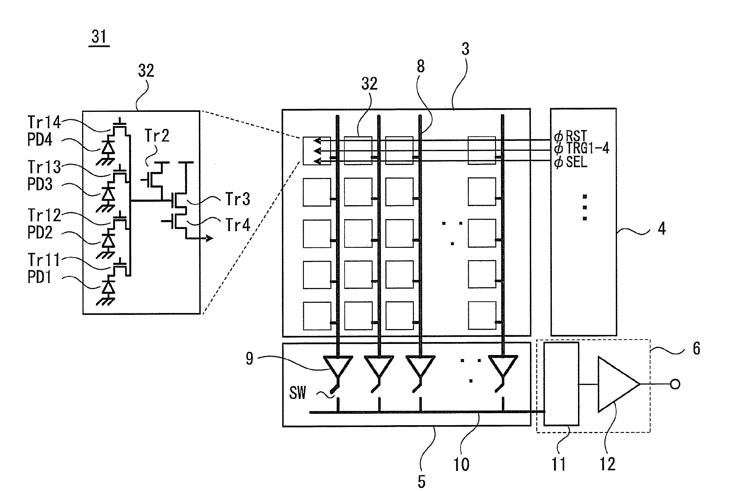
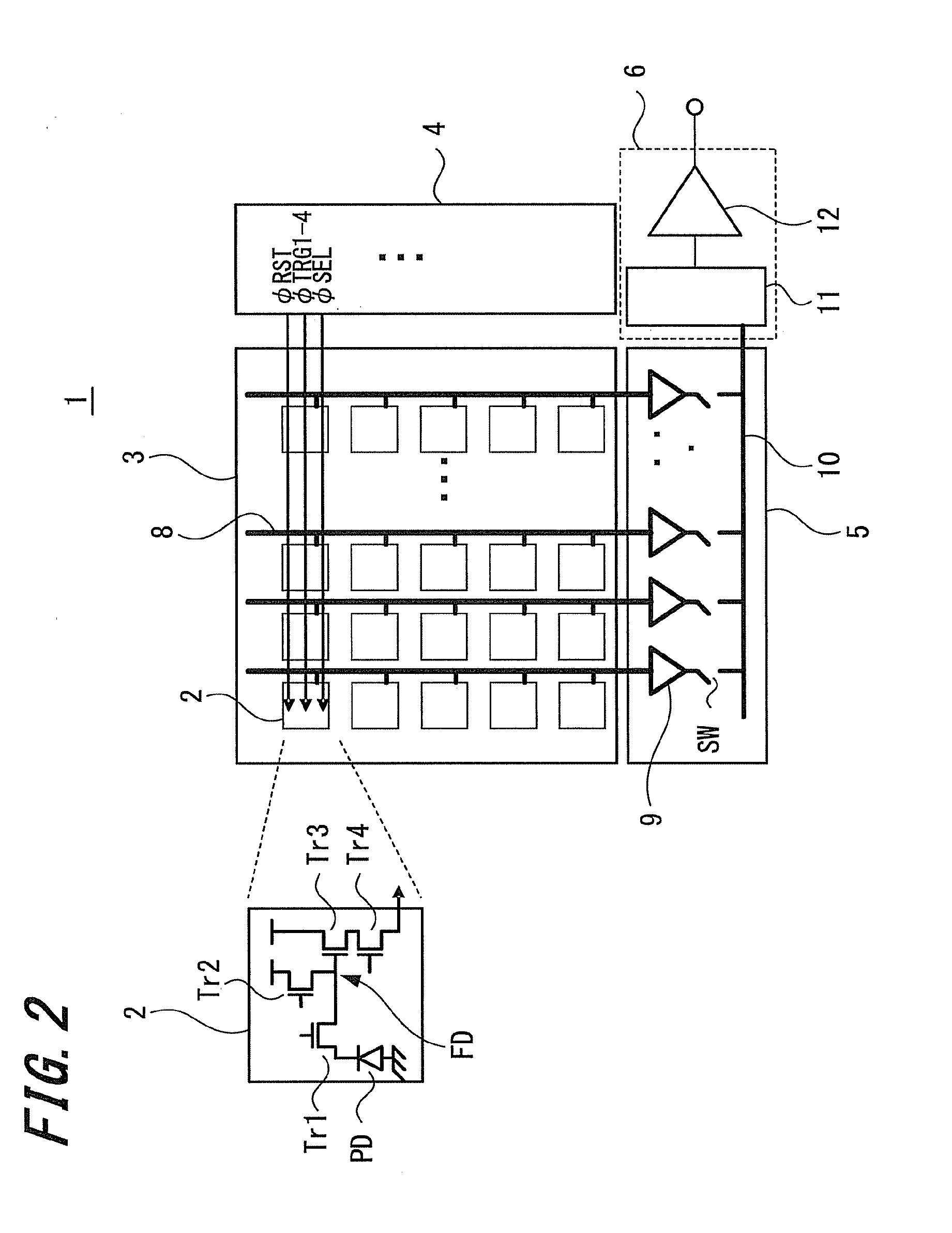
[0030]FIG. 2 is a schematic view illustrating a configuration of a solid-state imaging device or CMOS image sensor according to an embodiment of the present invention. Referring to FIG. 2, a solid-state imaging device 1 according to the present embodiment includes an imaging section 3 (i.e., pixel section) having a plurality of pixels 2 arranged in a two-dimensional array, and peripheral circuits arranged around the imaging section 3, having a vertical driving unit 4, a horizontal transfer unit 5, and an output unit 6. Each of the pixels 2 includes a photodiode PD serving as a photoelectric conversion element and several pixel transistors (MOS transistors) Tr.

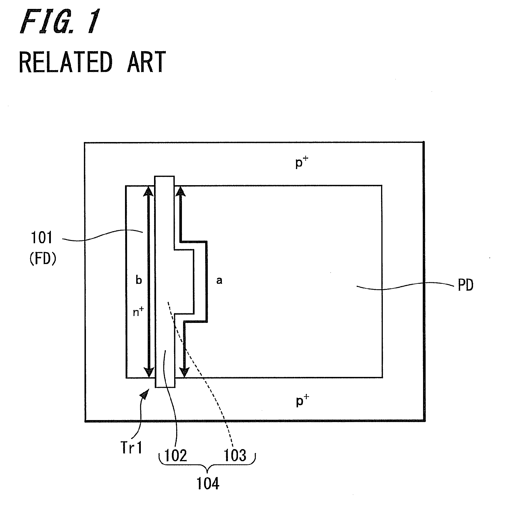
[0031]The photodiode PD includes a region configured to accumulate s...


PUM


Abstract

Disclosed is a solid-state imaging device which includes a plurality of pixels in an arrangement, each of the pixels including a photoelectric conversion element, pixel transistors including a transfer transistor, and a floating diffusion region, in which the channel width of transfer gate of the transfer transistor is formed to be larger on a side of the floating diffusion region than on a side of the photoelectric conversion element.

Description

CROSS REFERENCES TO RELATED APPLICATIONS[0001]The present invention contains subject matter related to Japanese Patent Application JP 2007-311183 filed in the Japanese Patent Office on Nov. 30, 2007, the entire contents of which being incorporated herein by reference.BACKGROUND OF THE INVENTION[0002]1. Field of the Invention[0003]The invention generally relates to solid-state imaging devices and cameras. More particularly, the invention relates to a solid-state imaging device and a camera provided with the solid-state imaging device.[0004]2. Description of the Related Art[0005]Solid-state imaging devices are classified broadly into amplification type solid-state imaging devices, which are typically exemplified by CMOS (complementary metal-oxide semiconductor) image sensors, and charge transfer type imaging devices, which are typified by CCD (charge-coupled device) image sensors.[0006]CMOS image sensors have replaced CCD sensors at rapid speed particularly in the area of portable dev...

Claims


Application Information

Patent Timeline
IPC IPC(8): H01L31/112H04N5/335H01L27/146H04N5/369H04N5/374
CPCH01L27/14603H01L27/14641H04N5/3745H01L27/14643H01L27/14614H01L27/1461H01L27/14616H04N25/76H04N25/77H04N25/75
Inventor KUDOH, YOSHIHARU
Owner SONY CORP
Why Eureka
Try Eureka