Light emitting element and electronic device using the same

Inactive Publication Date: 2009-06-04
SEMICON ENERGY LAB CO LTD
View PDF23 Cites 29 Cited by
  • Summary
  • Abstract
  • Description
  • Claims
  • Application Information

AI Technical Summary

Benefits of technology

[0025]Therefore, a light emitting element with lower hole injection barrier can be obtained by including a composite layer of the present application compared with a layer formed from only a material having low ionization potential. Further, a light emitting element in which a hole is easy to move can be obtained. In terms of such a function of the composite layer, the composite layer of the present application has a function like a hole generation layer or a hole transport layer in some cases.
[0026]Further, as described above, an electron is transferred even before voltage is applied in the composite layer employed in the present application; therefore, the composite layer is a film having extremely high conductivity. Thus, a light emitting element in which drive vol

Problems solved by technology

However, there is the following problem in the case of using metal oxide as a layer included in a light emitting element.
An electric field is concentrated in this projection and therefore a light emitting element having high reliability cannot be obtained.
In addition, there is another problem that drive voltage rises when a film thickness of metal oxide is increased for the purpose of preventing short-circuit between electrodes of a light emitting element due to dust or the like or for the purpose of optical design that light from a light emitting layer is efficiently extracted.
On the other hand, in the case of using an organic compound as a layer included in a light emitting element, drive voltage rises since holes are difficult to go into the organic compound If a material having a low

Method used


Image

  • Light emitting element and electronic device using the same
  • Light emitting element and electronic device using the same
  • Light emitting element and electronic device using the same

Examples


embodiment 1

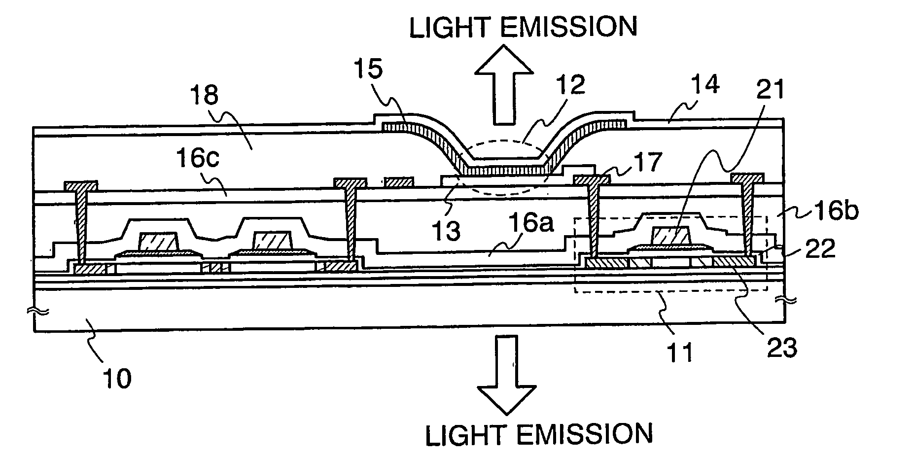
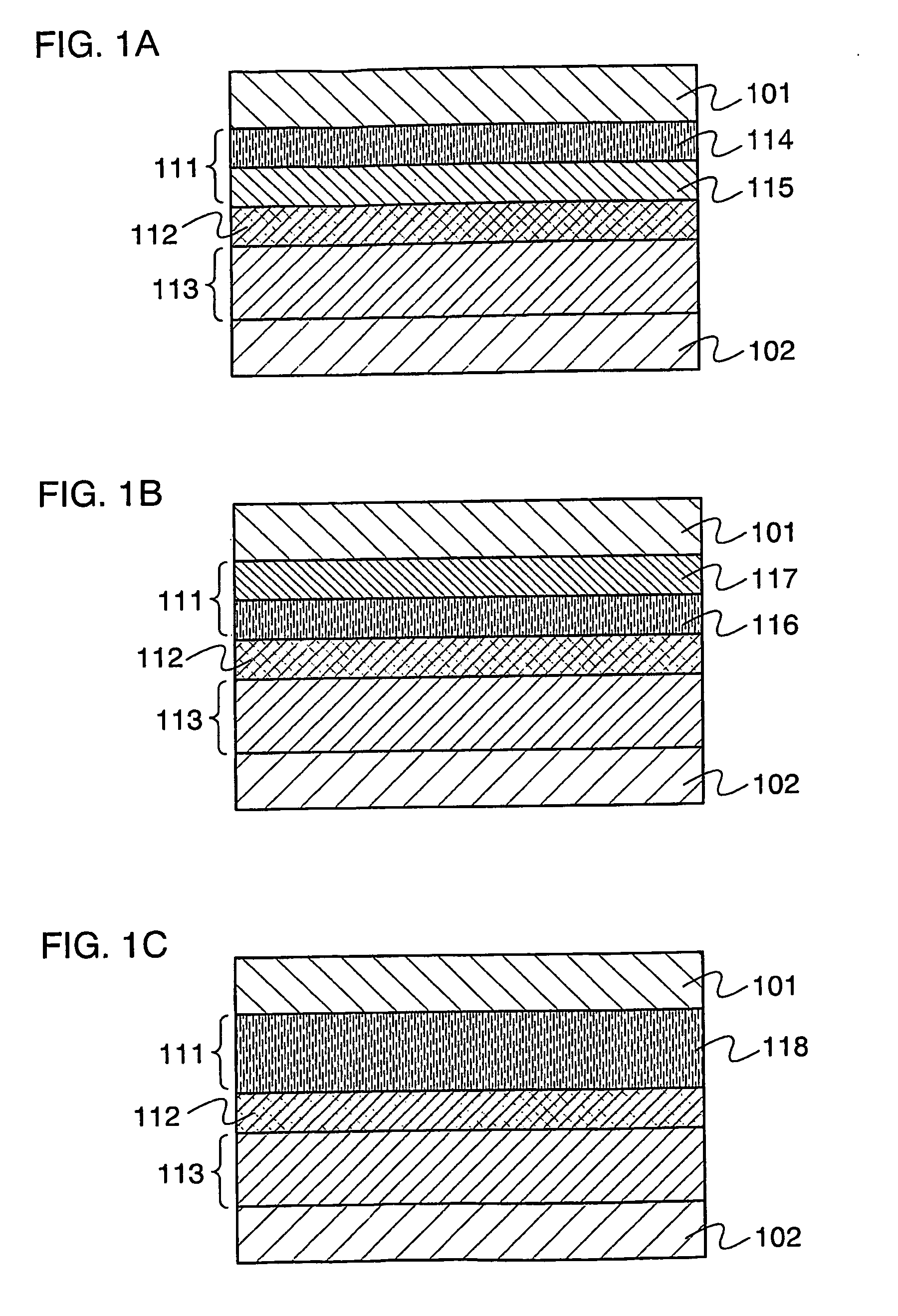
[0044]One mode of a light emitting element of the present invention is explained with reference to FIGS. 1A to 1C.

[0045]FIGS. 1A to 1C show a light emitting element including a first layer 111 which is in contact with a first electrode 101, a second layer 112 which is in contact with the first layer 111, and a third layer 113 which is in contact with the second layer 112 and a second electrode 102 between the first electrode 101 and the second electrode 102. In FIGS. 1A to 1C, light is emitted when voltage is applied to the electrode so that an electric potential of the first electrode 101 is higher than an electric potential of the second electrode 102. The second layer 112 is a light emitting layer, and the third layer 113 is a layer having a function of transporting or injecting an electron to the light emitting layer which is the second layer.

[0046]The second layer 112 contains a light emitting substance. The second layer 112 may be a layer formed from only a light emitting subs...

embodiment 2

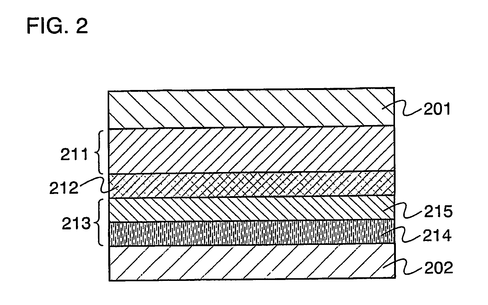
[0064]This embodiment is explained with reference to FIG. 2.

[0065]FIG. 2 shows a light emitting element including a first layer 211 which is in contact with a first electrode 201, a second layer 212 which is in contact with the first layer 211, and a third layer 213 which is in contact with the second layer 212 and a second electrode 202 between the first electrode 201 and the second electrode 202. The light emitting element in FIG. 2 emits light when voltage is applied so that an electric potential of the first electrode 201 is higher than an electric potential of the second electrode 202. The second layer 212 is a light emitting layer and the first layer 211 is a layer having a function of transporting or injecting a hole to the light emitting layer which is the second layer. The first layer may have a hole injecting layer or a hole transport layer. A material illustrated in Embodiment 1 can be used as a light emitting material, a material for the first electrode and the second el...

embodiment 3

[0072]In this embodiment, a multilayer structure between a second layer 112 and a first electrode 101 shown in Embodiment 1 and a multilayer structure between a second layer 212 and a second electrode 202 shown in Embodiment 2 are combined.

[0073]In this case, a composite layer is arranged between a first electrode and a light emitting layer and between a second electrode and the light emitting layer; accordingly, a light emitting element having higher conductivity and having a high hole injecting property or a high hole transporting property can be provided. In other words, a light emitting element having an advantage of Embodiment 1 and an advantage of Embodiment 2 is obtained.

[0074]FIGS. 3A to 3C show a light emitting element which is one mode of this embodiment. In FIGS. 3A to 3C, a second layer 312 which is a light emitting layer is arranged between a first electrode 301 and a second electrode 302, which are a pair of electrode; a first layer 311, between the first electrode 301...


PUM


Abstract

A layer included in an electroluminescent element is required to be thickened to optimize light extraction efficiency of the electroluminescent element and to prevent short-circuit between electrodes. However, in a conventional element material, desired light extraction efficiency cannot be accomplished since drive voltage rises or power consumption is increased as the element material is thickened. A composite is formed by mixing a conjugated molecule having low ionization potential and a substance having an electron-accepting property to the conjugated molecule. A composite layer included in an element is formed using the composite as an element material. The composite layer is arranged between a first electrode and a light emitting layer or between a second electrode and a light emitting layer. The composite layer has high conductivity; therefore, drive voltage does not rise even if a film thickness is increased. Thus, an electroluminescent element which can prevent short-circuit of an electrode can be provided.

Description

TECHNICAL FIELD[0001]The present invention relates to a light emitting element. More specifically, the invention relates to a light emitting element having a layer composed of a composite of a conjugated molecule and a substance having an electron-accepting property to the conjugated molecule. Further, the invention relates to a light emitting device including a light emitting element.BACKGROUND ART[0002]An electroluminescent (EL) display is one of the most remarkable devices as a flat panel display device for the next generation, which is composed of a light emitting element. In a light emitting element, electrons injected from a cathode and holes injected from an anode are recombined in a light emitting layer when current is flowed to form molecule excitons. The light emitting element emits light by using photons discharged when the molecular excitons return to the ground state. Therefore, one of conditions to manufacture a light emitting element having favorable emission efficien...

Claims


Application Information

Patent Timeline
IPC IPC(8): H01J1/63
CPCH01L51/0062H01L51/0094Y10S428/917H01L51/5052H01L51/5016H10K85/649H10K85/40H10K50/155H10K50/165H10K50/11H10K2101/10H05B33/00
Inventor NOMURA, RYOJISEO, SATOSHIABE, HIROKOTAKASU, TAKAKOINOUE, HIDEKOIKEDA, HISAOKUMAKI, DAISUKESAKATA, JUNICHIRO
Owner SEMICON ENERGY LAB CO LTD
Why Eureka
Try Eureka