Composite structure for microlithography and optical arrangement

a technology of optical arrangement and composite structure, applied in the field of composite structure for microlithography, can solve the problems of affecting the quality of the finished product, so as to achieve the effect of simple and cost-effective production

Inactive Publication Date: 2009-06-04
CARL ZEISS SMT GMBH
View PDF10 Cites 21 Cited by
  • Summary
  • Abstract
  • Description
  • Claims
  • Application Information

AI Technical Summary

Benefits of technology

[0008]It is one object of the invention to provide a composite structure for microlithography which can be produced simply and cost-effectively and in particular is suitable for lithography applications at high power density.SUBJECT MATTER OF THE INVENTION

Problems solved by technology

In microlithography, devices (e.g. wafer chuck, wafer stage, wafer table) are required, for example, for holding a wafer, and, although these can be implemented in part as monolithic, they are relatively heavy as a result of the overall sizes required there.
When such organic joining agents are used, pyrolysis and / or photolysis of the bond may occur in high-power applications, inter alia, on exposure to laser light in the UV or EUV wavelength range, e.g. at 193 nm, so that this becomes unstable.
Another problem is possibly also the matching of the refractive indices of the components as a result of the relatively thick boundary layer between the surfaces.

Method used


Image

  • Composite structure for microlithography and optical arrangement
  • Composite structure for microlithography and optical arrangement
  • Composite structure for microlithography and optical arrangement

Examples


Embodiment Construction

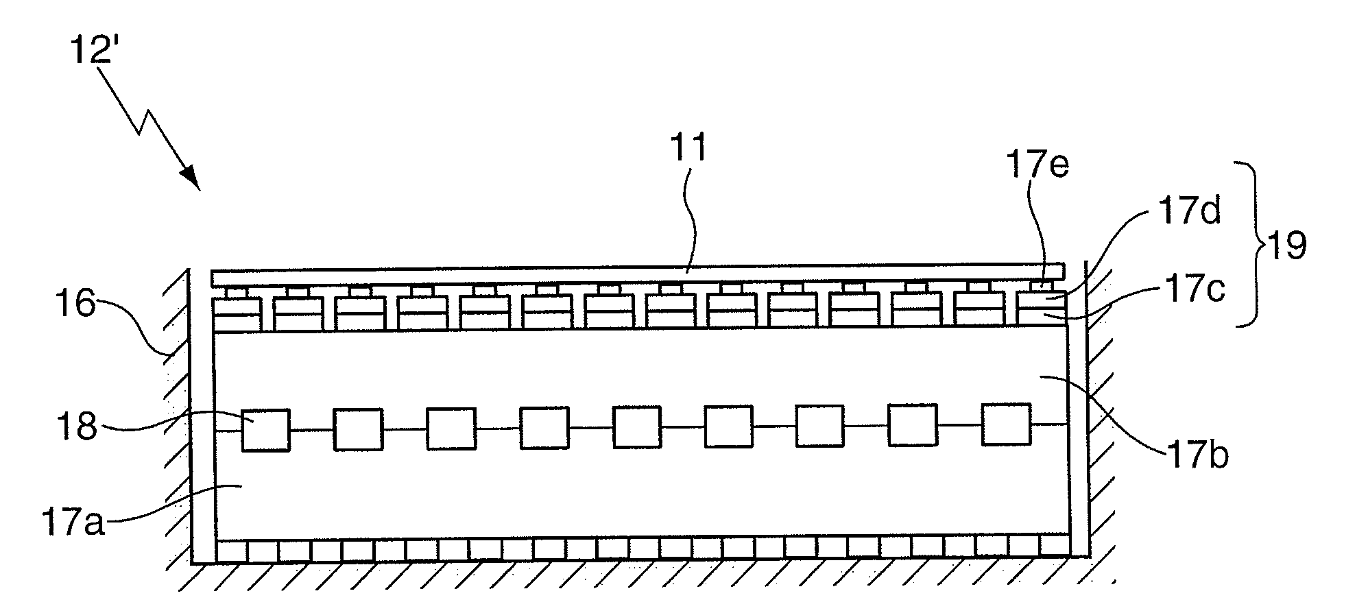
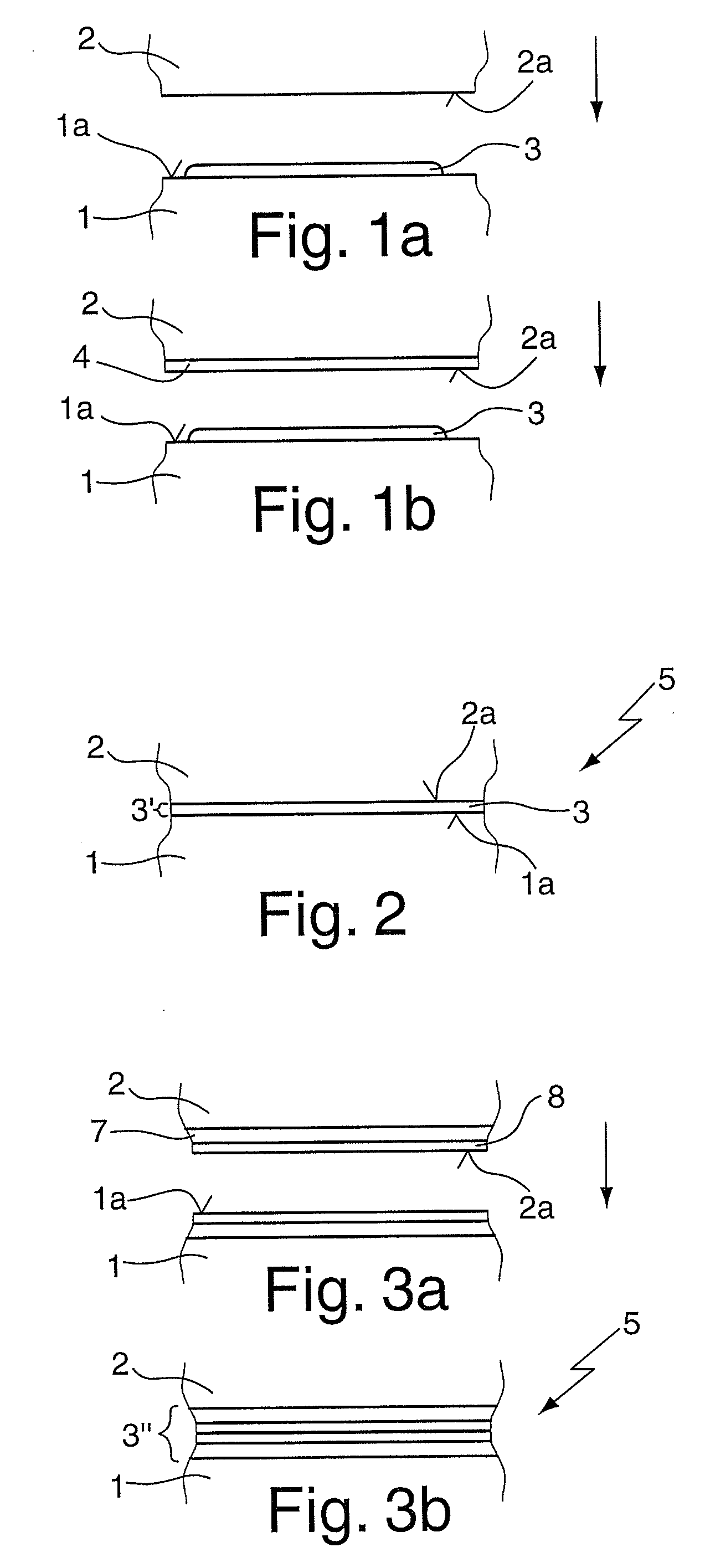
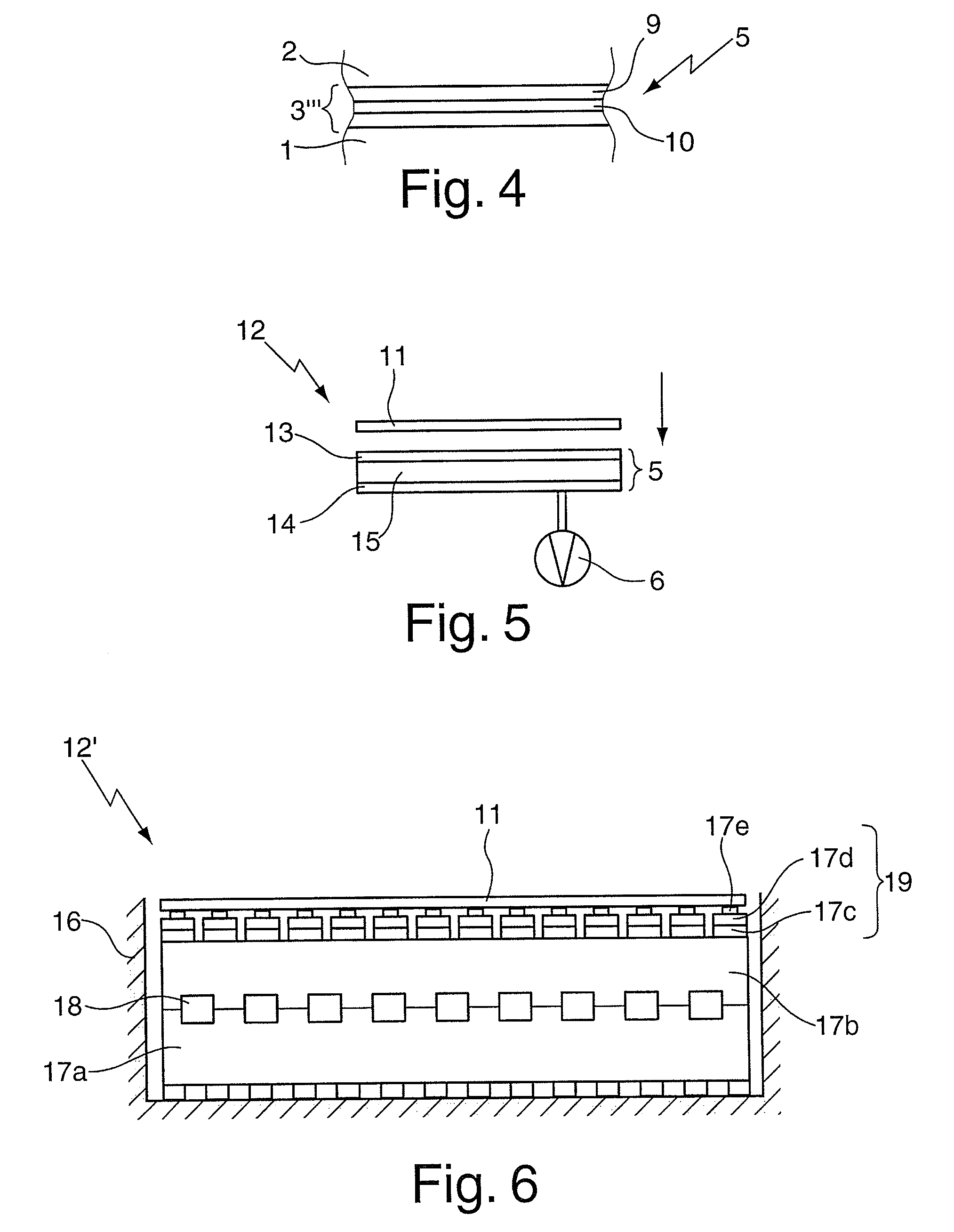
[0059]FIG. 1a is a schematic diagram of a first ceramic component 1 consisting of (poly)crystalline cordierite which has been produced in a sintering process, whereby this was obtained with high purity and therefore consists of a fraction higher than 98% of Mg2Al4Si5O18. Alternatively, naturally occurring mineral cordierite could also be used. A joining agent 3 is applied to a surface 1a of the cordierite component 1 to be joined, said joining agent 3 comprising an aqueous solution of polymerised silicic acid which was formed from monosilicic acid (H4SiO4). In this case, the polymerised silicic acid is mixed with at least one halogen. A chemical bond between the cordierite and another suitable material can be formed by the silicate-containing substance. Naturally, in addition to silicic acid and its derivatives, other silicate (SiO44−) suppliers can also be used, e.g. alkali silicates and / or alkali earth silicates or other silicate-containing substances such as are described, for ex...


PUM

PropertyMeasurementUnit
porosityaaaaaaaaaa
densityaaaaaaaaaa
temperatureaaaaaaaaaa

Abstract

A composite structure for microlithography, in particular a holding device for a wafer, has two or more components, the surfaces of which are bonded together at least at one bond. At least one of the components consists of cordierite (Mg2Al4Si5O18) or of silicon carbide (SiC). Also disclosed is an optical arrangement, in particular a projection illumination apparatus for microlithography, having at least one such composite structure, preferably a wafer stage.

Description

CROSS-REFERENCE TO RELATED APPLICATIONS[0001]This is a Continuation of International Application PCT / EP2007 / 006963, with an international filing date of Aug. 7, 2007, which was published under PCT Article 21(2) in English, and the complete disclosure of which, including amendments, is incorporated into this application by reference. This application claims priority under 35 U.S.C. 119(a) to German Patent Application No. 10 2007 005 780.8, filed on Feb. 6, 2007, and to German Patent Application No. 10 2006 037 629.3, filed on Aug. 10, 2006. The entire contents of each of these three applications are hereby incorporated into the present application by reference.FIELD OF AND BACKGROUND OF THE INVENTION[0002]The invention relates to a composite structure for microlithography, in particular a holding device for a wafer, comprising two or more components, the surfaces of which are bonded together at least at one bond. The invention further relates to a wafer stage and to an optical arrang...

Claims


Application Information

Patent Timeline
Patent Type & Authority Applications(United States)
IPC IPC(8): B32B18/00B32B3/26B32B15/04B32B17/06B32B3/12
CPCG03F7/707Y10T428/24661G03F7/7095H01L21/67103H01L21/68757Y10T428/12576C04B37/005C04B37/006C04B37/008C04B37/045C04B2235/77C04B2235/9607C04B2237/06C04B2237/062C04B2237/083C04B2237/10C04B2237/12C04B2237/121C04B2237/122C04B2237/123C04B2237/125C04B2237/341C04B2237/365C04B2237/52C04B2237/62C04B2237/708C04B2237/72G03F7/70858Y10T428/31678Y10T428/31612Y10T428/249953
Inventor EKSTEIN, CLAUDIAHOLDERER, HUBERT
Owner CARL ZEISS SMT GMBH
Why Eureka
Try Eureka