Method and on-chip control apparatus for enhancing process reliability and process variability through 3D integration

a technology of process reliability and process variability, applied in the field of control methods and on-chip controllers for enhancing semiconductor chip process variability and lifetime reliability, can solve the problems of limiting the applicability of methods in practice, increasing complexity, and increasing the cost of process variation in technologies, so as to facilitate the implementation of methods, improve the design of integrated circuits, and alleviate lifetime reliability and process variability problems.

Inactive Publication Date: 2009-06-04
GLOBALFOUNDRIES INC
View PDF19 Cites 207 Cited by
  • Summary
  • Abstract
  • Description
  • Claims
  • Application Information

AI Technical Summary

Benefits of technology

[0008]In essence, the present invention is directed to providing an on-chip controller adapted to facilitate implementing a method to alleviate lifetime reliability and process variability issues through three-dimensional integration. Three-dimensional integration has shown significant potential for improving the integrated circuit design in the past years. Even though the motivations for 3D has been largely interconnect driven and packaging, 3D integration can provide further advantages if it is effectively utilized.
[0009]Concerning the foregoing, the invention is directed to a method for enhancing the lifetime reliability and process variability through effective use of three-dimensional integration technology. An auxiliary so-called healing layer is attached to an original processor die through 3D integration. This one-fits-all auxiliary layer can solve any reliability or variability problem automatically at run time, and preserves the synchronous timing while potentially improving the performance of a faulty chip compared to the baseline. Proposed is an intelligent on-chip controller which manages the redundancy in the auxiliary layer, including exact replicas of number of critical blocks; generic and configurable logic resources; configurable wiring and high-bandwidth low-latency interconnect to the primary layer. The invention, thus, focuses on utilizing these resources through 3D integration in order to improve upon lifetime reliability and variability, but not claiming the invention of an additional device layer or the hardware units in this layer.
[0010]A primary aspect of the invention resides in utilizing the available 3D redundancy, by dynamically adjusting the processor resources on both layers, i.e., primary and device layers, simultaneously including logic and interconnectivity in order to bring the system to a state at which it can achieve at least the same or improved performance over the baseline. High-end server systems are good candidates for this “healing / compensating layer technique”. Not only does the additional memory hierarchy in this layer provide performance improvement, the reconfigurable redundancy enables enhanced lifetime reliability in recovering from a wide range of faults.
[0011]The auxiliary or second device layer includes: (i) an on-chip reliability / variability controller, which is capable of monitoring on-chip resources, recovering from faults and process variability induced differences through activating / deactivating / configuring one or more of the logic or memory units or interconnect on the chip; (ii) exact replicas of critical blocks on the second layer (whereby both layers have matching floor plans, where the duplicates are located vertically on top of the originals), but not all units in a microprocessor are of equal criticality. Units such as register files, issue or fetch logic are of higher importance compared to caches and predictors, for which faults can be tolerated to a certain extent; (iii) generic logic, which is to be used as redundancy for various reconfigurable redundancy enables enhanced lifetime reliability recovering from a wide range of faults.

Problems solved by technology

Increased requirements in power density and technology scaling for electronic package components have encountered considerably increased existing reliability problems in recent years, as a result of which lifetime reliability and process variation have already been elevated to the “critical challenges” category according to ITRS [ITRS05] in the technology.
The utilization of structural duplication is considered as another standard technique for dealing with lifetime reliability issues; however, the corresponding required overhead in terms of increased cost, manufacturing area and complexity, generally limits the extent of applicability thereof in practice.
Similarly, the traditional burn-in process that is used to accelerate extrinsic failures is reaching a point where it is raising a number of complications and is becoming more difficult to implement with each successive process generation.
In some instances, burn-in is believed to cause lifetime reliability problems itself, as a result of which, there has been an increased degree of interest in developing alternative techniques for improving the chip lifetime reliability without the burn-in process in recent years.
There is a significant amount of cost associated with the process variation in technologies, especially at levels of 32 nm and below.
Lost yield due to process variability causes millions of dollars in wasted expenditures every year per production line.
There is significant cost and problems associated with lost yield due to process variation in current and next generation technologies.
These include timing and associated functionality problems, performance reduction due to the timing changes, increase in chip footprint due to the additional blocks, ability to handle only single fault and single type of fault due to lack of intelligence in the current approaches to dealing with variability.

Method used


Image

  • Method and on-chip control apparatus for enhancing process reliability and process variability through 3D integration
  • Method and on-chip control apparatus for enhancing process reliability and process variability through 3D integration
  • Method and on-chip control apparatus for enhancing process reliability and process variability through 3D integration

Examples


Embodiment Construction

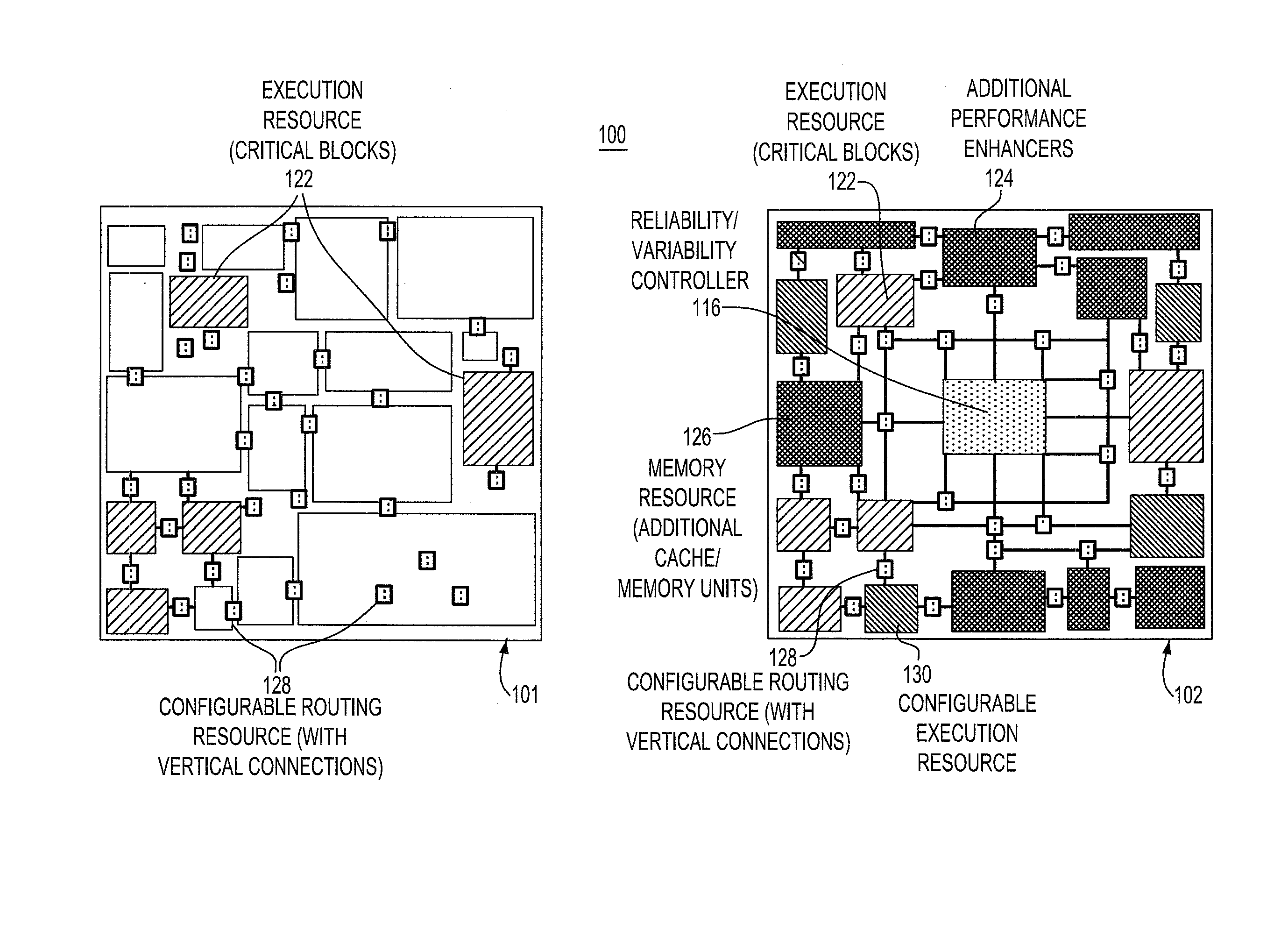
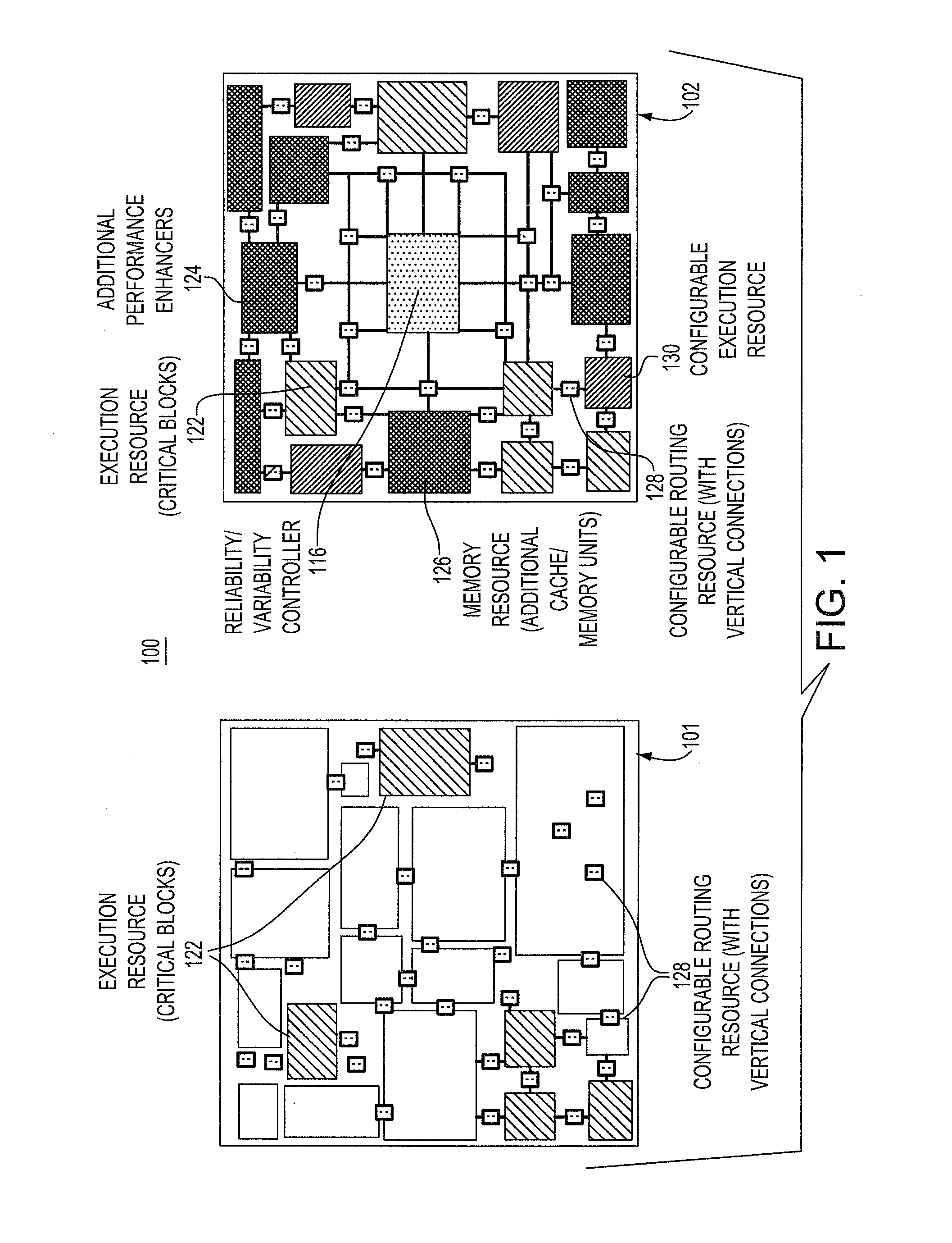
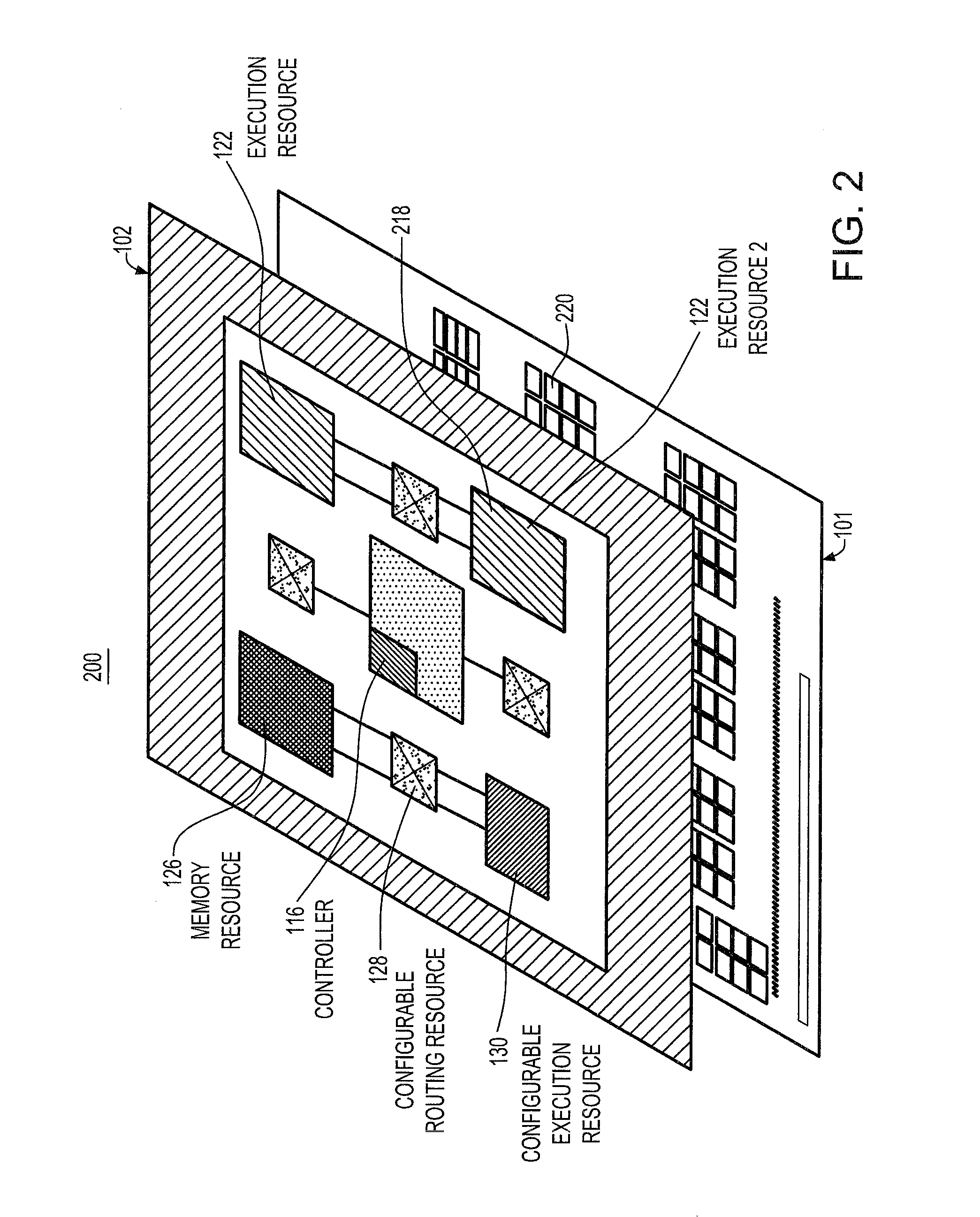
[0017]Pursuant to the method for enhancing lifetime reliability and / or performance that uses 3D integration, there are employed at least two chips where the first chip is a microprocessor. The second chip consists of a set of execution / memory resources configurable as either redundant resource for the microprocessor and microcontroller for managing and reconfiguring the resources in response to detection of a need for replacing a resource in the first chip in a sequence of steps where as a first step the pool of existing execution or memory resources is scanned to find an eligible replacement for the resource marked for replacement. If the eligible resource is not available, one of the reconfigurable resources is configured to replace the resource that is marked for replacement. Hereby, one or more of the execution / memory resources in the second chip is configured to work as a performance enhancer for one of the resources in the first chip (such as a second pipeline in the auxiliary...


PUM


Abstract

A method and on-chip controller for enhancing semiconductor chip process variability and lifetime reliability through a three-dimensional (3D) integration applied to electronic packaging. Also provided is an on-chip reliability/variability controller arrangement for implementing the inventive method.

Description

BACKGROUND OF THE INVENTION[0001]1. Field of the Invention[0002]The present invention relates to a control method and on-chip controller for enhancing semiconductor chip process variability and lifetime reliability through the intermediary of three-dimensional (3D) integration.[0003]2. Background of the Invention[0004]Increased requirements in power density and technology scaling for electronic package components have encountered considerably increased existing reliability problems in recent years, as a result of which lifetime reliability and process variation have already been elevated to the “critical challenges” category according to ITRS [ITRS05] in the technology.[0005]Chip lifetime reliability has traditionally been ensured through process qualification and sorting out of defective chips through accelerated degradation techniques like process burn-in. The utilization of structural duplication is considered as another standard technique for dealing with lifetime reliability is...

Claims


Application Information

Patent Timeline
Patent Type & Authority Applications(United States)
IPC IPC(8): G06F9/45
CPCG06F2201/845G06F11/2023
Inventor BOSE, PRADIPKURSUN, ERENRIVERS, JUDE A.ZYUBAN, VICTOR
Owner GLOBALFOUNDRIES INC
Why Eureka
Try Eureka