Method of Fabricating Flash Memory Device

a flash memory and device technology, applied in the direction of semiconductor devices, basic electric elements, electrical appliances, etc., can solve the problems of low film quality characteristics, low efficiency, and increased leakage current, so as to improve film quality characteristics, high performance, and step coverage characteristics

Inactive Publication Date: 2009-06-25
SK HYNIX INC
View PDF2 Cites 2 Cited by
  • Summary
  • Abstract
  • Description
  • Claims
  • Application Information

AI Technical Summary

Benefits of technology

[0007]The present invention is directed towards a method of fabricating a flash memory device. A dielectric layer, having a stacked structure of an oxide layer, a nitride layer, and an oxide layer, may be formed using a plasma oxidization process in a state where a back bias voltage is applied to at least one oxide layer. A result is that a step coverage characteristic and a film quality characteristic can be improved, while forming a thick oxide layer. Therefore a dielectric layer with high performance and high reliability can be formed.

Problems solved by technology

Thus, if it sought to store data at a low program voltage within a short period of time, the ratio of voltage applied to the control gate electrode and voltage induced to the floating gate has to be great.
However, if the thickness of the dielectric layer reduces, the leakage current increases and a charge retention characteristic is reduced, degrading the characteristics of devices.

Method used


Image

  • Method of Fabricating Flash Memory Device
  • Method of Fabricating Flash Memory Device
  • Method of Fabricating Flash Memory Device

Examples


Embodiment Construction

[0022]Now, specific embodiments of the present invention will be described with reference to the accompanying drawings. However, the present invention is not limited to the disclosed embodiments, but may be implemented in various ways. The embodiments are provided to complete the disclosure of the present invention and to allow those having ordinary skill in the art to understand the scope of the present invention. The present invention is defined by the category of the claims.

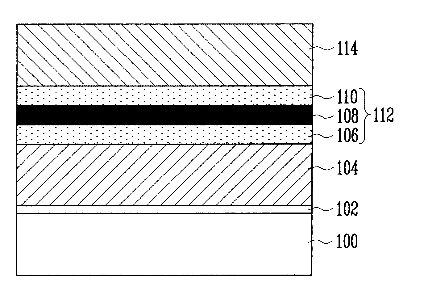
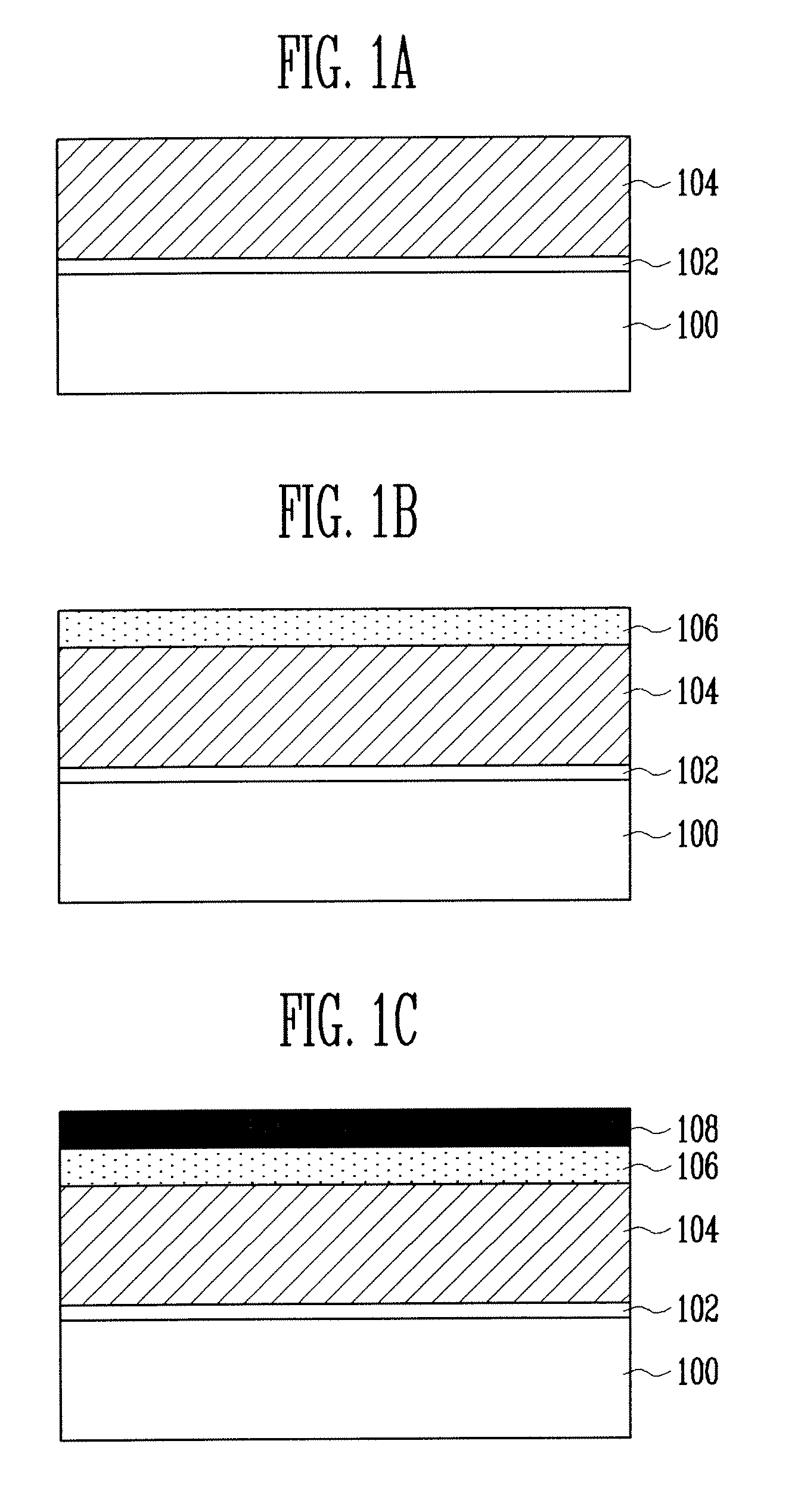
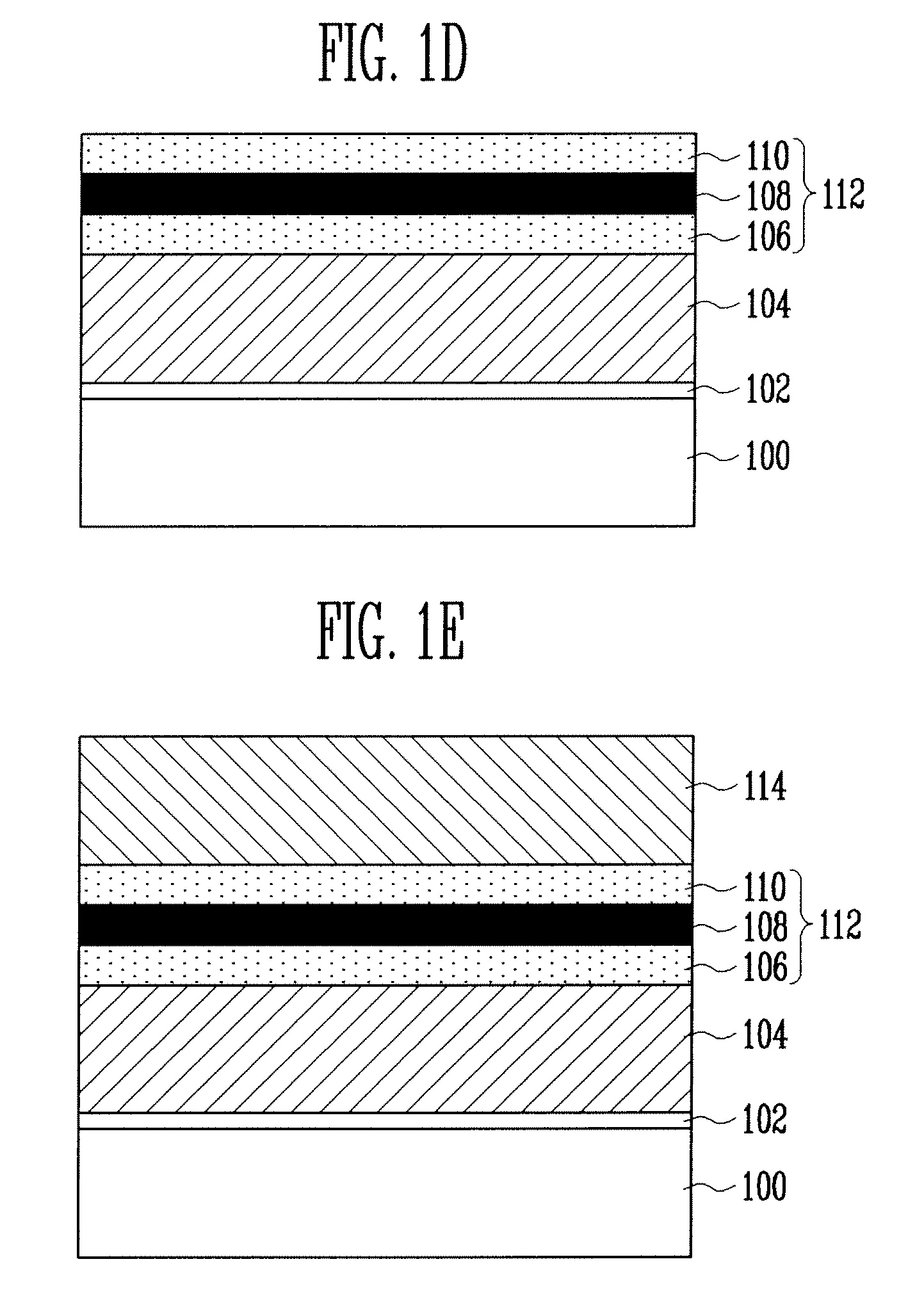
[0023]FIGS. 1A to 1E are sectional views illustrating a method of fabricating a flash memory device in accordance with embodiments of the present invention.

[0024]Referring to FIG. 1A, a semiconductor substrate 100 in which a well area (not shown) is formed is provided. The well area can have a triple structure. The well area is formed by forming a screen oxide layer (not shown) on the semiconductor substrate 100 and then performing a well ion implantation process and a threshold voltage ion implantation proces...


PUM


Abstract

The present invention relates to a method of fabricating a flash memory device. According to a method of fabricating a flash memory device in accordance with an aspect of the present invention, a semiconductor substrate over which a tunnel insulating layer and a first conductive layer are formed is provided. A first oxide layer is formed on the first conductive layer using a plasma oxidization process in a state where a back bias voltage is applied. A nitride layer is formed on the first oxide layer. A second oxide layer is formed on the nitride layer. A second conductive layer is formed on the second oxide layer.

Description

CROSS-REFERENCES TO RELATED APPLICATION[0001]The present application claims priority to Korean patent application number 10-2007-0119658, filed on Nov. 22, 2007, which is incorporated by reference in its entirety.BACKGROUND OF THE INVENTION[0002]The present invention relates to a method of fabricating a flash memory device and, more particularly, to a method of fabricating a flash memory device, in which, in a state where a back bias voltage is applied, an oxide layer of a dielectric layer is formed using a plasma oxidization process.[0003]In general, non-volatile memory devices retain data stored therein when power is off. A unit cell of this non-volatile memory device includes a tunnel insulating layer, a floating gate, a dielectric layer, and a control gate all of which are sequentially stacked over an active area of a semiconductor substrate. The unit cell can store data as voltage from the outside to a control gate electrode is coupled to the floating gate. Thus, if it sought t...

Claims


Application Information

Patent Timeline
Patent Type & Authority Applications(United States)
IPC IPC(8): H01L21/28
CPCH01L27/11521H01L21/28273H01L29/40114H10B41/30H01L21/02252
Inventor PARK, EUN SHILHONG, KWONKIM, JAE HONGKOO, JAE HYOUNG
Owner SK HYNIX INC
Why Eureka
Try Eureka