High power light emitting diode package and manufacturing method thereof

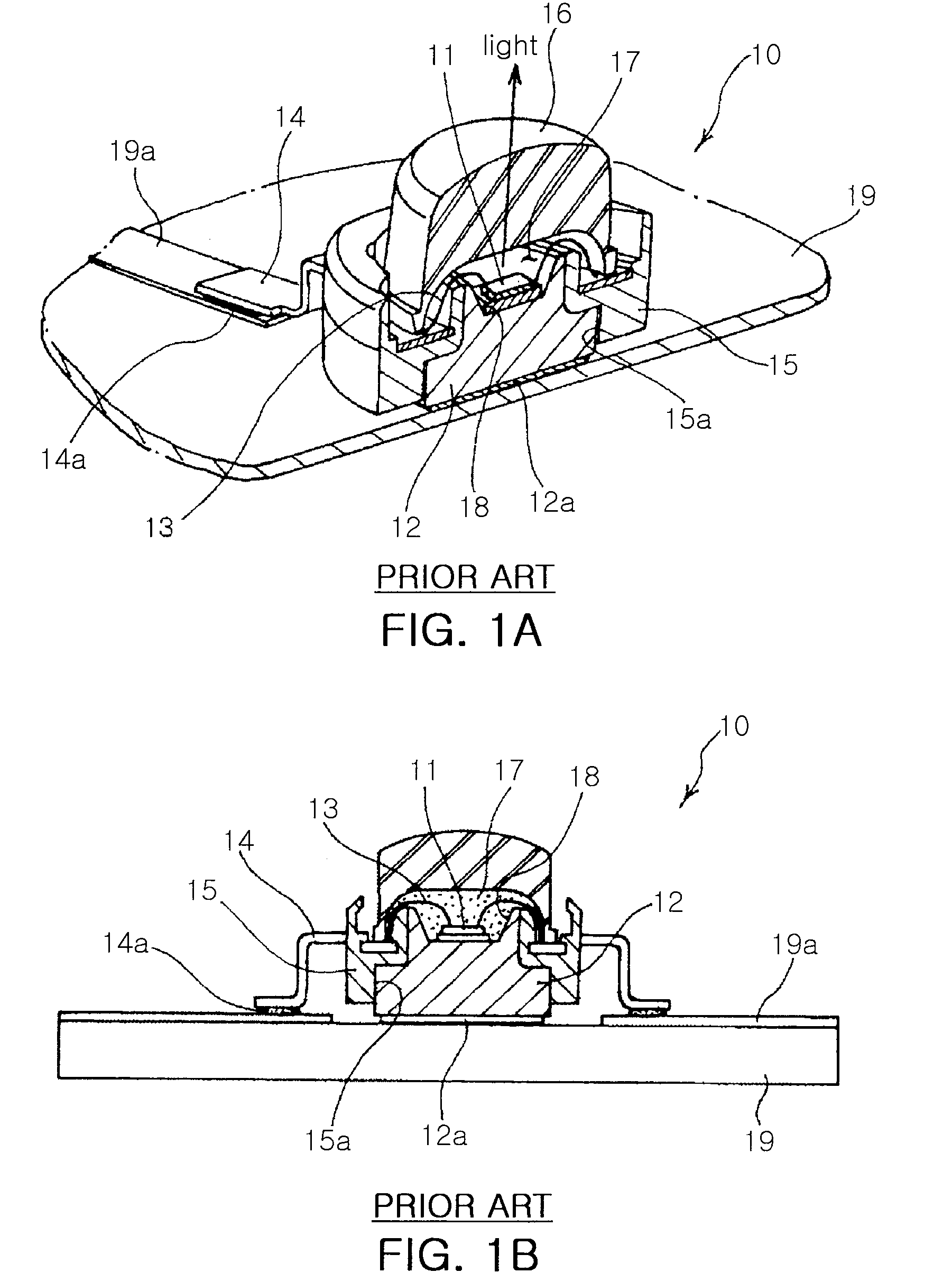
a technology of light-emitting diodes and manufacturing methods, which is applied in the direction of semiconductor/solid-state device manufacturing, electrical apparatus, semiconductor devices, etc., can solve the problems of increasing manufacturing costs, destroying led packages b>10/b> with repeated thermal impact, and degrading thermal characteristics of conventional led packages

Inactive Publication Date: 2009-07-02
SAMSUNG ELECTRONICS CO LTD
View PDF6 Cites 96 Cited by
  • Summary
  • Abstract
  • Description
  • Claims
  • Application Information

AI Technical Summary

Benefits of technology

[0052]The heat radiator may further include a lens part or a molding part formed of a transparent material to protect the light emitting chip from external environment.
[0053]The heat radiator may include: an encapsulant formed on the chip

Problems solved by technology

However, the conventional LED package 10 with this structure may be degraded in thermal characteristics since the molding part 15 made of polymer may be deteriorated at a high temperature.
Besides, the LED package 10 may be ruined by repeated the

Method used


Image

  • High power light emitting diode package and manufacturing method thereof
  • High power light emitting diode package and manufacturing method thereof
  • High power light emitting diode package and manufacturing method thereof

Examples


Embodiment Construction

[0072]Exemplary embodiments of the present invention will now be described in detail with reference to the accompanying drawings.

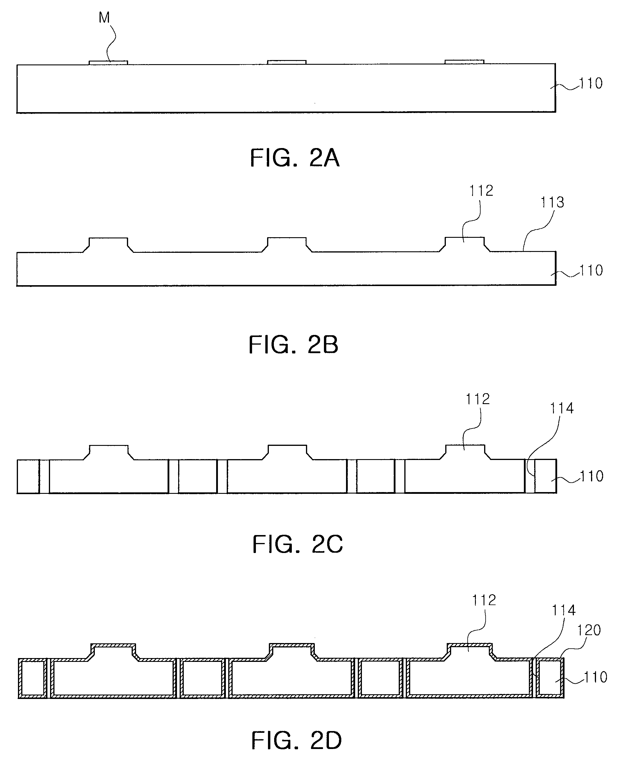
[0073]FIGS. 2A to 2I are cross-sectional views illustrating a method of manufacturing a high power LED package according to an exemplary embodiment of the invention. FIGS. 3A to 3H are perspective views illustrating a method of manufacturing a high power LED package according to an exemplary embodiment of the invention.

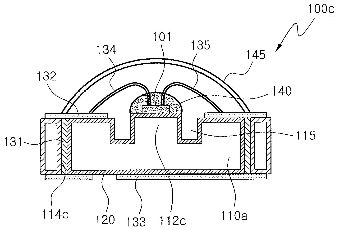
[0074]The high power LED package 100 of the present embodiment is manufactured by following processes of a to e.

[0075]a. At Least One Chip Mounting Part and at Least One Via Hole are Formed on a Metal Plate.

[0076]As shown in FIGS. 2A to 2C and FIGS. 3A to 3C, a metal plate 110 having a predetermined size is provided thereon with chip mounting parts 112 where light emitting chips 101 are mounted, respectively upon application of a power source and through holes 114 for forming conductive via holes.

[0077]As shown in FIG. 2A and FIG. 3A, the me...


PUM


Abstract

There is provided a high power LED package and a method of manufacturing the same. The method includes: forming at least one chip mounting part and at least one through hole in a metal plate; forming an insulating layer of a predetermined thickness on an entire outer surface of the metal plate; forming an electrode part to be electrically connected to a light emitting chip mounted on the chip mounting part; and cutting the metal plate along a trimming line to separate the package. The LED package is free from thermal impact resulting from different thermal coefficients among components, thus ensuring stable heat radiation characteristics in a high temperature atmosphere. Also, the LED package is minimized in optical loss to improve optical characteristics. In addition, the LED package is simplified in a manufacturing and assembly process and thus can be manufactured in mass production at a lower cost.

Description

CROSS-REFERENCE TO RELATED APPLICATIONS[0001]This application claims the priorities of Korean Patent Application Nos. 2007-0140549 filed on Dec. 28, 2007 and 2008-0097213 filed on Oct. 2, 2008, in the Korean Intellectual Property Office, the disclosures of which are incorporated herein by reference.BACKGROUND OF THE INVENTION[0002]1. Field of the Invention[0003]The present invention relates to a high power light emitting diode package and a manufacturing method of the same.[0004]2. Description of the Related Art[0005]In general, a light emitting diode (LED) is a semiconductor device emitting light when current flows, and a PN junction diode formed of a GaAs or GaN optical semiconductor which converts an electrical energy into a photonic energy.[0006]The light emitted from this LED ranges from red light spectrum (630 nm to 700 nm) to blue-violet light spectrum (400 nm), thus encompassing blue, green and white light spectrums. The LED is lower in power consumption, higher in efficienc...

Claims


Application Information

Patent Timeline
IPC IPC(8): H01L33/00H01L21/24H01L33/44H01L33/48
CPCH01L33/44H01L33/486H01L33/62H01L2224/73265H01L24/97H01L2924/12041H01L2224/48247H01L2224/8592H01L2224/48091H01L2924/00014H01L2924/00H01L33/641H01L2924/12036H01L2924/181H01L2924/00012
Inventor PARK, JUNG KYUKO, KUN YOOPARK, YOUNG SAMCHOL, SEUNG HWANKIM, IL KU
Owner SAMSUNG ELECTRONICS CO LTD
Why Eureka
Try Eureka