Semiconductor device and die bonding material

a semiconductor device and die bonding technology, applied in semiconductor devices, solid-state devices, basic electric elements, etc., can solve the problems of mechanical strength degradation of joints, increased production costs, and insufficient die bonding materials of lead-tin solder and tin-antimony solder, so as to secure the mountability and electrical reliability of semiconductor devices, the effect of good melting temperatur

Inactive Publication Date: 2009-07-02
PANASONIC CORP
View PDF15 Cites 4 Cited by
  • Summary
  • Abstract
  • Description
  • Claims
  • Application Information

AI Technical Summary

Benefits of technology

[0012]An object of the present invention is to provide an inexpensive bonding material which has a satisfactory melting temperature of, for example, at least 280° C. and is lead-free, and to secure the mountability and electrical reliability of a semiconductor device.

Problems solved by technology

A solder material containing tin as a composition forms an intermetallic compound layer with a metal of a bonded material, and the intermetallic compound layer changes with time and causes mechanical strength degradation on a joint.
However, of die bonding materials for a semiconductor element of the prior art, lead-tin (Pb—Sn) solder and tin-antimony (Sn—Sb) solder contain lead (Pb) and antimony (Sb) as metals and are not expected to be used as die bonding materials in the future.
Thus lead-tin solder and tin-antimony solder are not proper as die bonding materials.
However, solder using silver (Ag) and gold (Au), which are expensive metals, is an expensive die bonding material and thus increases the production cost.

Method used


Image

  • Semiconductor device and die bonding material
  • Semiconductor device and die bonding material
  • Semiconductor device and die bonding material

Examples


first embodiment

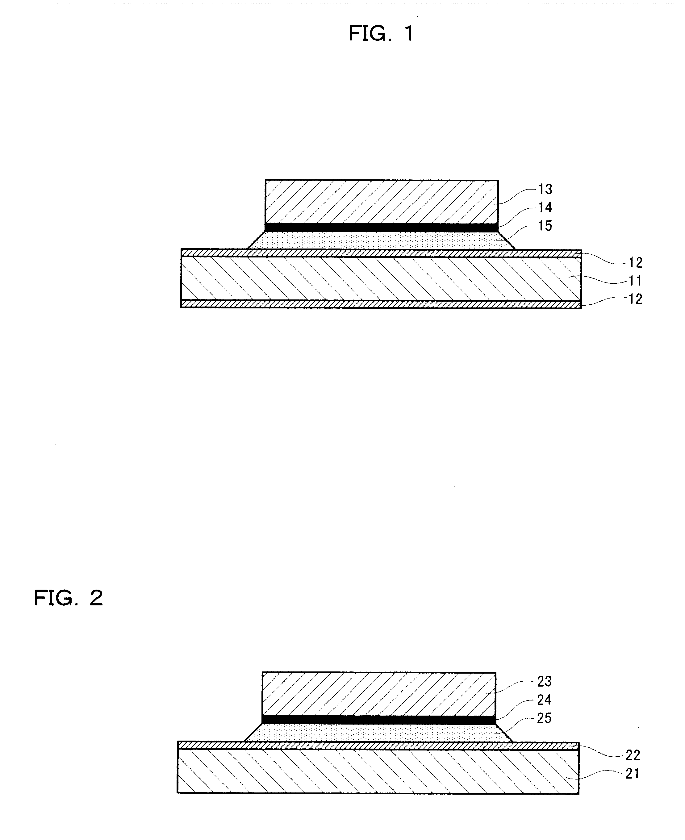
[0033]A bonding material which is a die bonding material for bonding a semiconductor element according to the present embodiment contains an alloy predominantly composed of Bi. The alloy contains 0.8 wt % to 10 wt % of Cu and 0.02 wt % to 0.2 wt % of Ge. It is known that a melting point increases as a larger amount of Cu having a melting point of 1083° C. is applied to the alloy predominantly composed of Bi having a melting point of 270° C. In order to evenly apply 0.8 wt % to 10 wt % of Cu as an alloy, it is necessary to prevent Cu particles from growing in size by temporarily melting Cu in a melting pot at 1200° C. and increasing the cooling speed. Further, a preferable Cu content is 0.8 wt % to 3.8 wt % and a preferable Ge content is 0.02 wt % to 0.05 wt %. When the alloy predominantly composed of Bi is a ternary alloy (an alloy composed of three elements), the residue other than Cu and Ge is only composed of Bi.

[0034]Such a bonding material has a melting temperature of at least ...

second embodiment

[0046]A bonding material that is a die bonding material according to the present embodiment contains an alloy predominantly composed of Bi. The alloy contains 0.8 wt % to 10 wt % of Cu, 0.02 wt % to 0.2 wt % of Ge, and 0.02 wt % to 0.08 wt % of Ni. As in the first embodiment, a preferable Cu content is 6 wt % to 10 wt % and a preferable Ge content is 0.02 wt % to 0.05 wt %. Further, a Ni content of 0.02 wt % to 0.05 wt % is preferable. By adding Ni thus, shock resistance becomes higher than in the bonding material of the first embodiment.

[0047]The shock resistance can be evaluated by a test in which a weight of 60 g is caused to collide, from a height of 180 mm, against a side of a chip capacitor having a size of 1.6 mm×0.8 mm.

[0048]The shock resistance test was conducted using the chip capacitor having a joint bonded with a ternary alloy (Bi-0.5% Cu-0.04% Ge) containing 99.46 wt % of Bi, 0.5 wt % of Cu, and 0.04 wt % of Ge. As a result, the joint of the chip capacitor was broken. W...

third embodiment

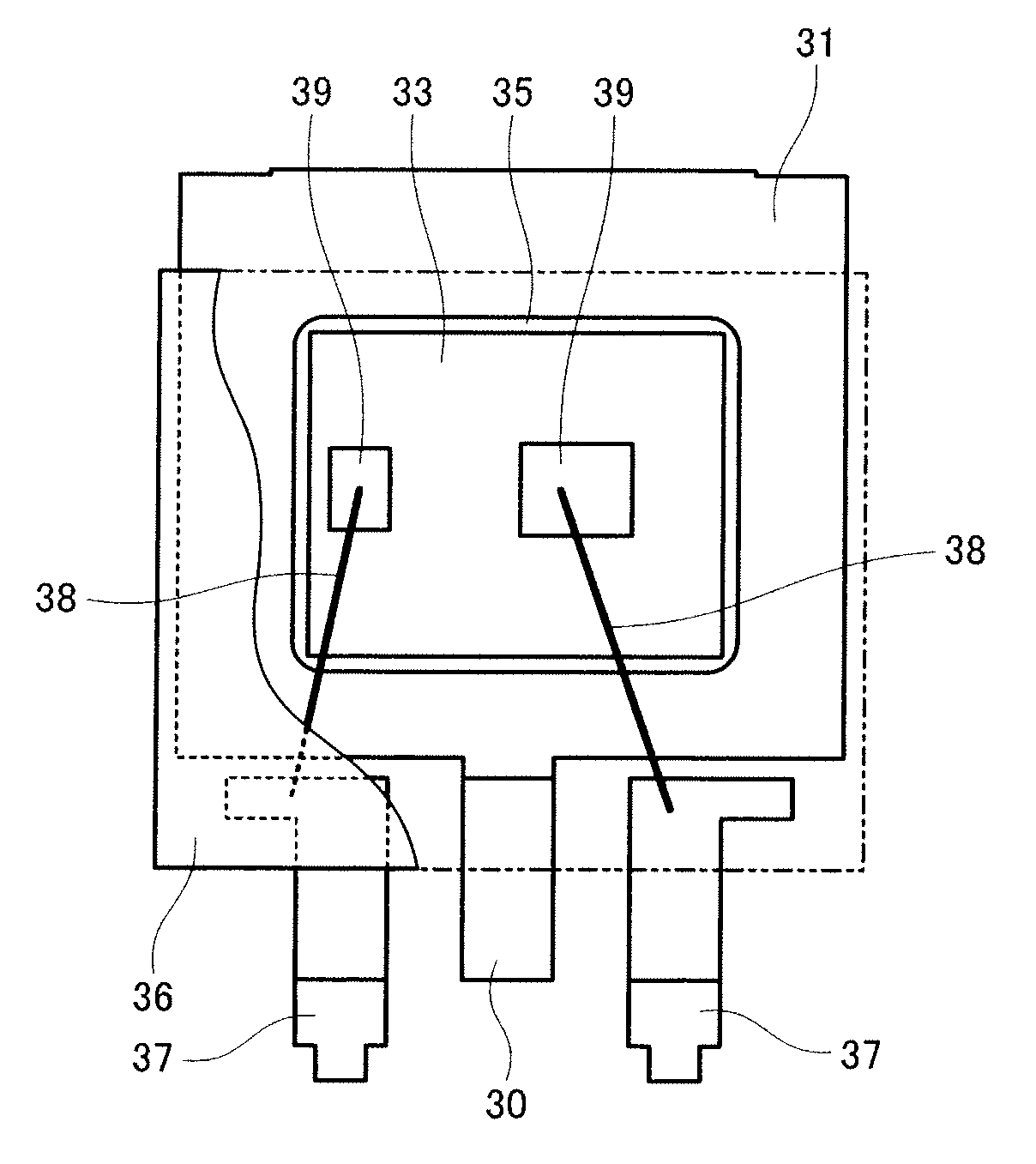
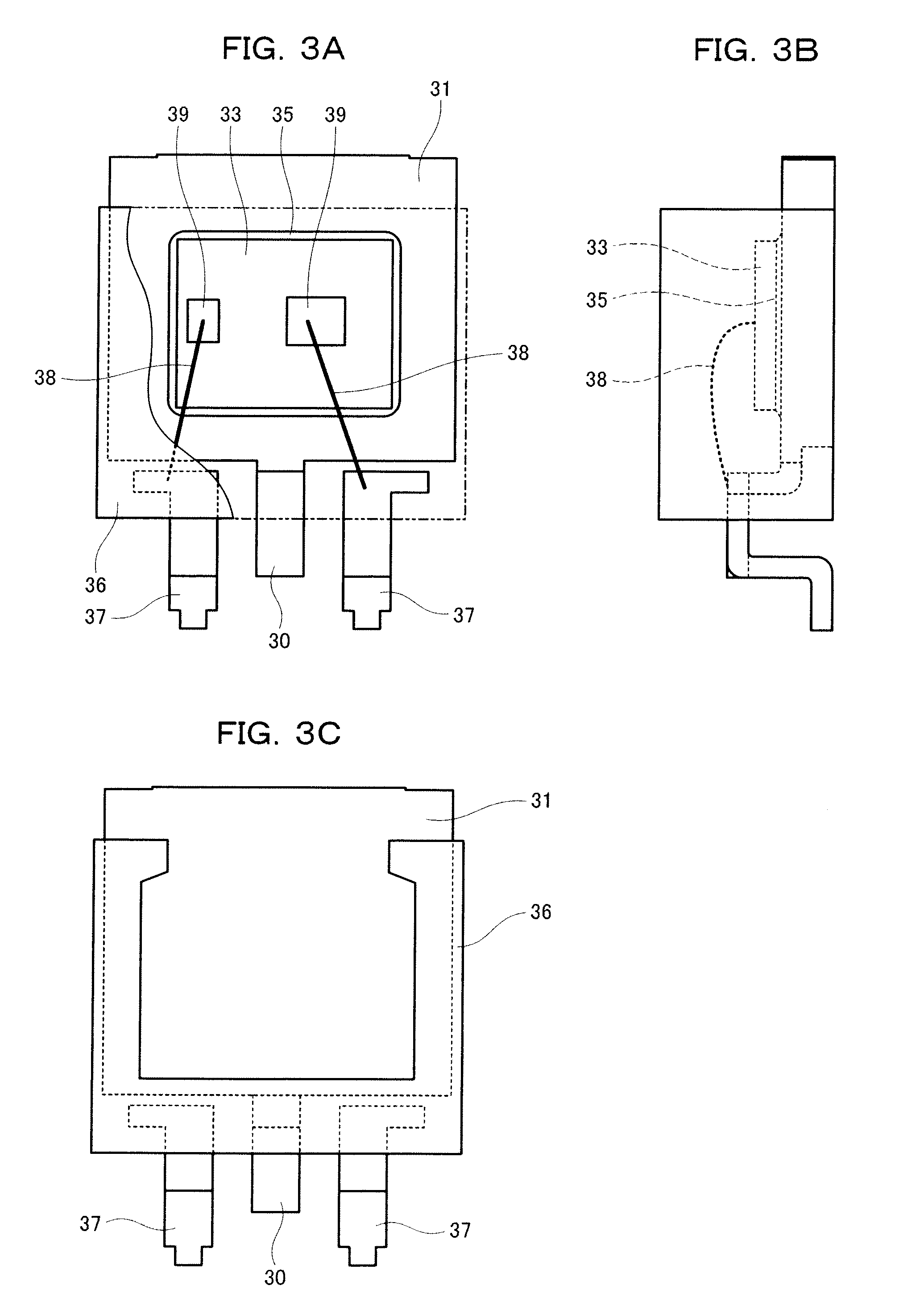
[0054]According to a semiconductor device of the present embodiment, when a semiconductor element having at least one semiconductor element backside electrode is mounted on a semiconductor substrate having at least one semiconductor substrate electrode, the semiconductor element and the semiconductor substrate are bonded to each other with the bonding material, which is a die bonding material according to one of the first and second embodiments, such that the semiconductor element backside electrodes and the corresponding semiconductor substrate electrodes are electrically connected to each other.

[0055]The semiconductor element is not particularly limited. For example, a semiconductor device for power may be used. Further, the semiconductor element may be a module as well as a single unit and particularly, a surface-mount device may be used.

[0056]The present invention is especially suitable when a semiconductor element for power is obtained with a size of not larger than 4.5 mm×7.6 ...


PUM


Abstract

In a semiconductor device bonded to a motherboard with a bonding material having a melting point of 200° C. to 230° C., a bonding material 15 which is a die bonding material for bonding a semiconductor element 13 to a semiconductor substrate 11 is a Bi alloy containing 0.8 wt % to 10 wt % of Cu and 0.02 wt % to 0.2 wt % of Ge, so that the bonding material 15 for bonding the semiconductor element 13 to the semiconductor substrate 11 is not melted when the semiconductor device is bonded to the motherboard by reflowing. It is therefore possible to suppress poor connection on the semiconductor element 13, thereby securing the mountability and electrical reliability of the semiconductor device.

Description

FIELD OF THE INVENTION[0001]The present invention relates to a die bonding material used for bonding a semiconductor element and a semiconductor substrate, and a semiconductor device using the die bonding material.BACKGROUND OF THE INVENTION[0002]A semiconductor element mounted on a semiconductor substrate includes electrodes electrically connected to a semiconductor substrate having external terminal electrodes, and a bonding material used for bonding is generally a solder material. In die bonding of the semiconductor element, attention should be given to the elemental components of a die bonding material. When die-bonding the semiconductor element, it is necessary to select a die bonding material which is electrically connected to the semiconductor substrate without inclining the semiconductor element or causing voids.[0003]The semiconductor device is mounted on a motherboard with another bonding material that is generally a solder material having a melting point of 200° C. to 230...

Claims


Application Information

Patent Timeline
Patent Type & Authority Applications(United States)
IPC IPC(8): H01L23/48C22C12/00
CPCH01L2224/29111H01L2224/04042H01L24/29H01L24/32H01L2224/0603H01L2224/32245H01L2224/48091H01L2224/73265H01L2924/01013H01L2924/01029H01L2924/01032H01L2924/01047H01L2924/01049H01L2924/0105H01L2924/01051H01L2924/01079H01L2924/01082H01L2224/29H01L2224/29298H01L2924/01005H01L2924/01006H01L2924/01019H01L2924/01033H01L2924/01075H01L2924/01322H01L2924/014H01L2224/29101H01L2924/0132H01L2224/48247H01L2924/0133H01L2924/01327H01L2924/0134H01L2224/83455H01L2224/29113H01L2924/00013H01L24/05C22C12/00H01L2924/00014H01L2924/00H01L2924/00012H01L2924/01028H01L2924/01083H01L2924/3512H01L2224/29099H01L2224/29199H01L2224/29299H01L2224/2929H01L24/73H01L2924/181
Inventor FUJIWARA, SEIJITOMITA, YOSHIHIROFURUSAWA, AKIOSUETUGU, KENICHIROU
Owner PANASONIC CORP
Why Eureka
Try Eureka