Strained-channel fet comprising twist-bonded semiconductor layer

a twist-bonded semiconductor and strain-channel technology, which is applied in the field of strain-channel fets, can solve the problems of increasing difficulty in maintaining trend, and achieve the effects of improving twist-bonded semiconductor layer properties, higher carrier mobility, and critical thickness

Inactive Publication Date: 2009-07-09
GLOBALFOUNDRIES INC +1
View PDF7 Cites 28 Cited by
  • Summary
  • Abstract
  • Description
  • Claims
  • Application Information

AI Technical Summary

Benefits of technology

[0011]In this invention, the properties of the twist-bonded semiconductor layer are exploited in a new way. Previously the deformation of the twist-bonded semiconductor layer in response to the stress of an epitaxially-grown, lattice-mismatched semiconductor overlayer was used to provide a benefit for the overlayer (i.e., a higher critical thickness). In the present invention, the deformation of the twist-bonded semiconductor layer in response to one or more locally applied stress elements is used to improve the properties of the twist-bonded semiconductor layer itself (i.e., to provide a higher carrier mobility). While the same stress elements will also cause a deformation (

Problems solved by technology

This trend is becoming increasingly more difficult to mai

Method used


Image

  • Strained-channel fet comprising twist-bonded semiconductor layer
  • Strained-channel fet comprising twist-bonded semiconductor layer
  • Strained-channel fet comprising twist-bonded semiconductor layer

Examples


Embodiment Construction

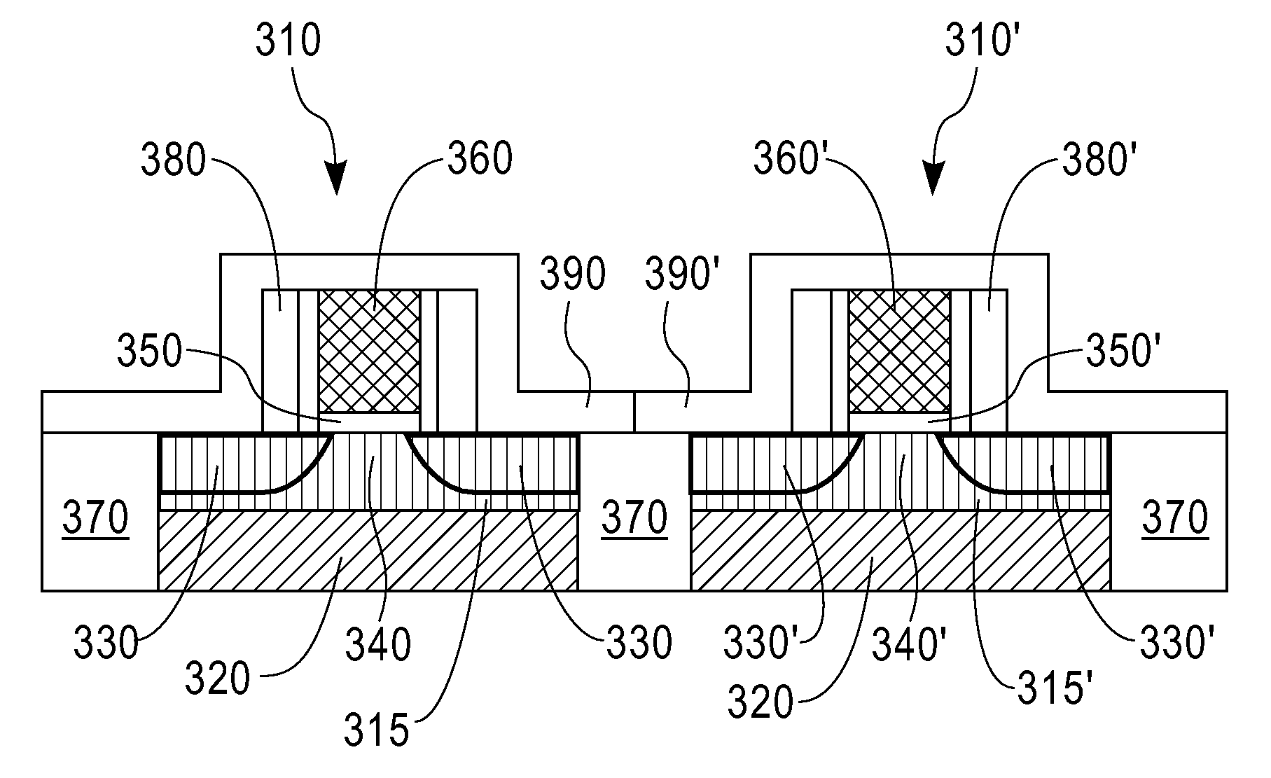
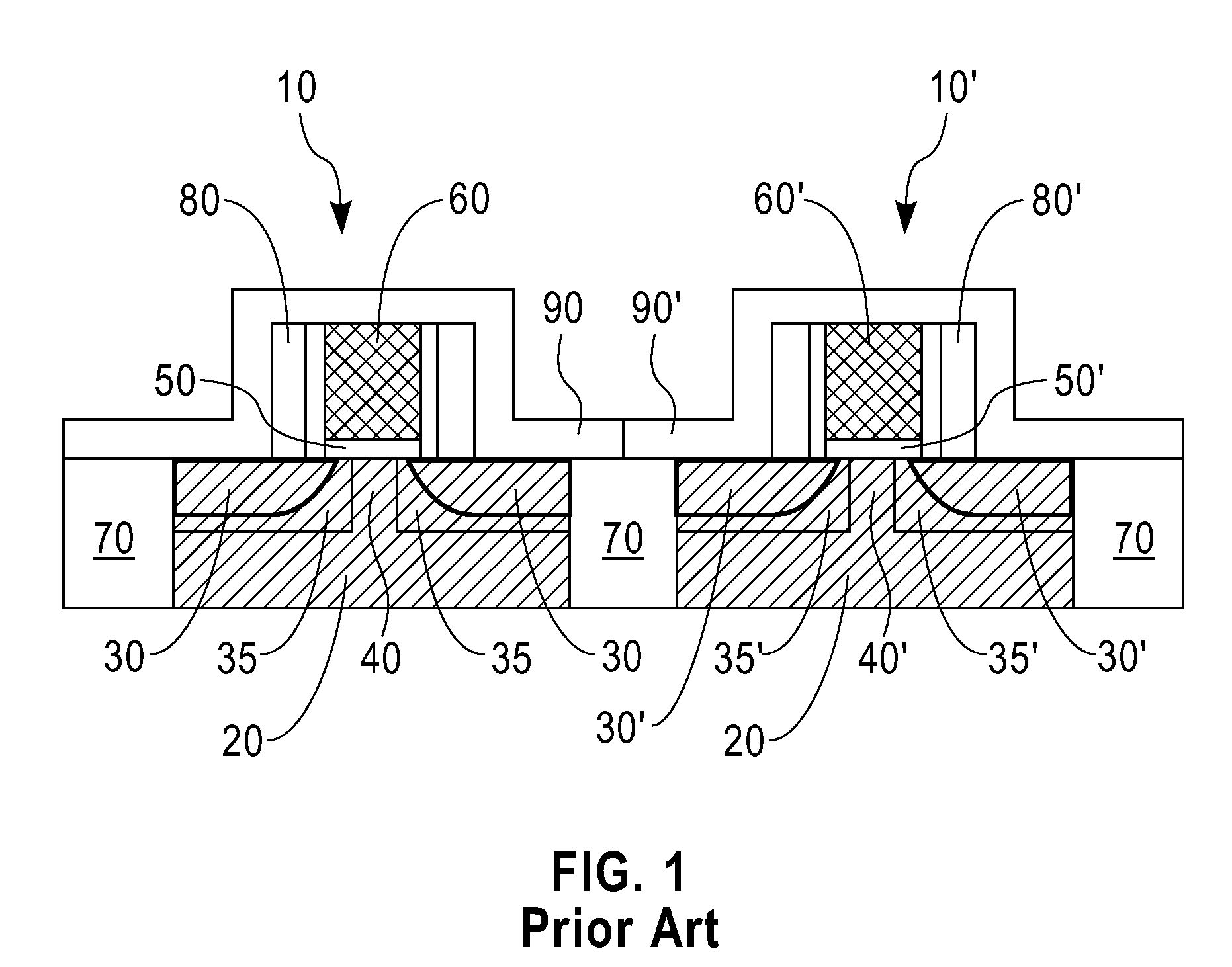
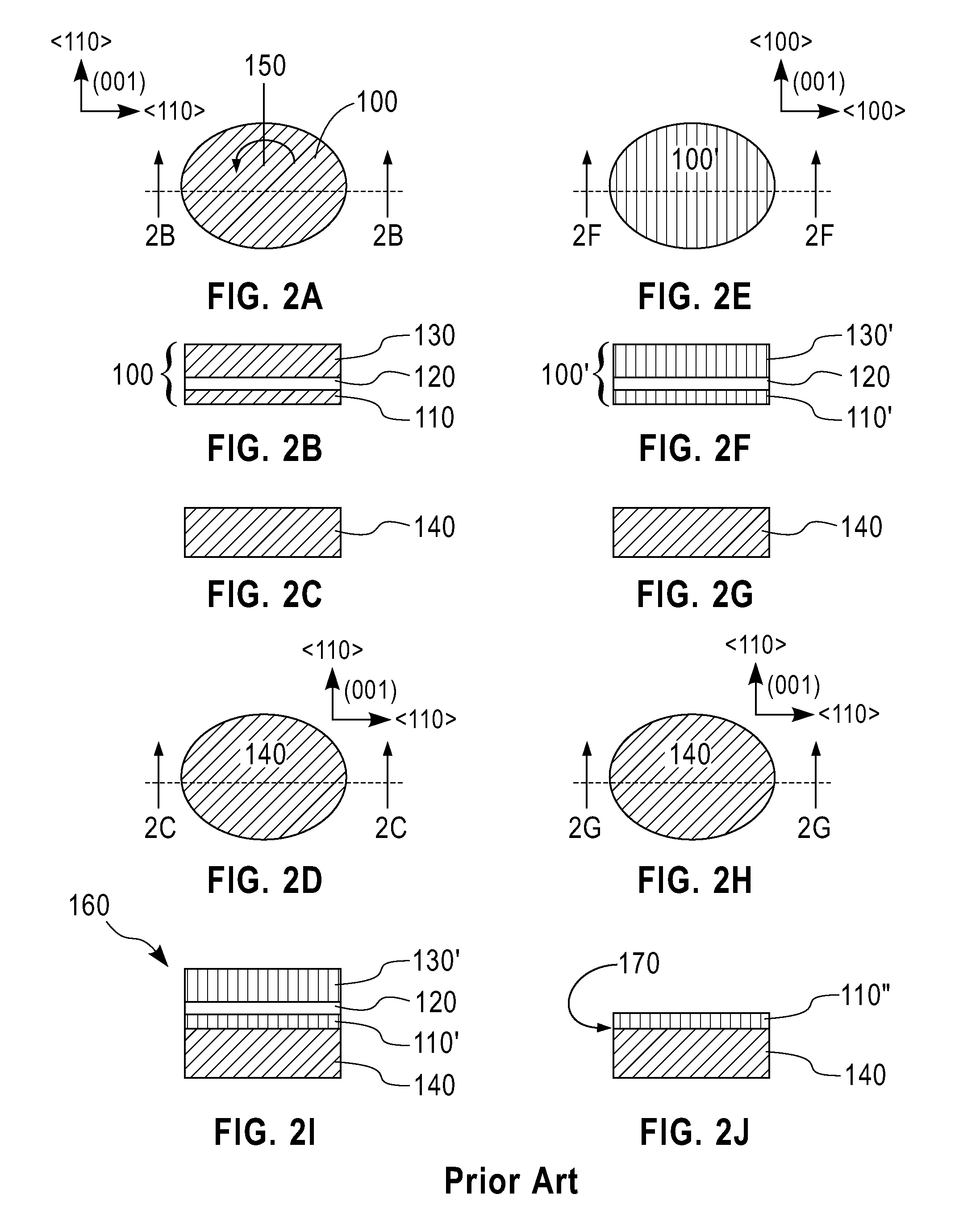
[0026]The present invention, which provides a semiconductor structure including at least one FET including a strained semiconductor channel disposed in a twist-bonded semiconductor layer in which at least some channel strain is induced by one or more local stress elements known in the art and related methods of forming the same, will now be described in greater detail by referring to the following discussion and drawings that accompany the present application. It is noted that the drawings of the present application are provided for illustrative purposes only and, as such, the drawings are not drawn to scale.

[0027]In the following description, numerous specific details are set forth, such as particular structures, components, materials, dimensions, processing steps and techniques, in order to provide a thorough understanding of the present invention. However, it will be appreciated by one of ordinary skill in the art that the invention may be practiced without these specific details...


PUM


Abstract

This invention provides a strained-channel field effect transistor (FET) in which the semiconductor of the channel of the FET is formed in a compliant substrate layer disposed over a twist-bonded semiconductor interface. This FET geometry increases the efficacy of local stress elements such as stress liners and embedded lattice-mismatched source/drain regions by mechanically decoupling the semiconductor of the channel region from the underlying rigid substrate. These strained-channel FETs may be incorporated into complementary metal oxide semiconductor (CMOS) circuits in various combinations. In one embodiment of this invention, both pFETs and nFETs are in a twist-bonded (001) silicon layer on a (001) silicon base layer. In another embodiment, pFETs are in a twist-bonded (011) silicon layer on a (001) silicon base layer and nFETs are in a conventional, non-twist-bonded (001) silicon base layer. This invention also provides a twist-bonded semiconductor layer on a polycrystalline base layer, as well as methods for fabricating the aforementioned FETs.

Description

FIELD OF THE INVENTION[0001]This invention generally relates to field effect transistors (FETs) in which at least some channel strain is induced by one or more local stress elements, such as, for example, stress liners and / or lattice-mismatched embedded source / drain regions. More particularly, this invention relates to increasing the effectiveness of such local stress elements by forming the FET channel region in a compliant semiconductor layer disposed over a twist-bonded semiconductor interface.BACKGROUND OF THE INVENTION[0002]Historically, most performance improvements in semiconductor field effect transistors (FETs) have been achieved by scaling down the relative dimensions of the device. This trend is becoming increasingly more difficult to maintain as the devices reach their physical scaling limits. As a consequence, advanced FETs and the complementary metal oxide semiconductor (CMOS) circuits in which they can be found are increasingly utilizing strain engineering to achieve ...

Claims


Application Information

Patent Timeline
IPC IPC(8): H01L29/04H01L21/20H01L21/8238H01L27/092H01L29/778
CPCH01L21/76251H01L21/823807H01L21/823878H01L21/84H01L27/0922H01L29/7849H01L29/045H01L29/165H01L29/7843H01L29/7848H01L27/1203
Inventor HAMAGUCHI, MASAFUMIHASUMI, RYOJIYIN, HAIZHOUSAENGER, KATHERINE L.
Owner GLOBALFOUNDRIES INC
Why Eureka
Try Eureka