Semiconductor Die Packages Having Overlapping Dice, System Using the Same, and Methods of Making the Same

Active Publication Date: 2009-07-09
SEMICON COMPONENTS IND LLC
View PDF19 Cites 13 Cited by
  • Summary
  • Abstract
  • Description
  • Claims
  • Application Information

AI Technical Summary

Benefits of technology

[0003]As part of making their invention, the inventors have recognized that the above-distributed two-stage power-conversion topology suffers from a lower overall power-conversion efficiency due, in part, to parasitic capacitances and inductances in the interconnect wires that electrically interconnect the converter's switching transistors. The inventors have further recognized that the buck converters used in the above-described configuration typically have duty-cycles substantially less than 50%, and therefore the size of the high-side power device (i.e., the device that charges the buck inductor from the intermediate DC voltage) may be significantly smaller than the low-side power device (i.e., the device that provides the synchronous free-wheeling rectifier). Because of the size difference and low duty cycle, the dice for the high-side and low-side devices may be incorporated in

Problems solved by technology

While this configuration has many advantages, it has a disadvanta

Method used


Image

  • Semiconductor Die Packages Having Overlapping Dice, System Using the Same, and Methods of Making the Same
  • Semiconductor Die Packages Having Overlapping Dice, System Using the Same, and Methods of Making the Same
  • Semiconductor Die Packages Having Overlapping Dice, System Using the Same, and Methods of Making the Same

Examples


Embodiment Construction

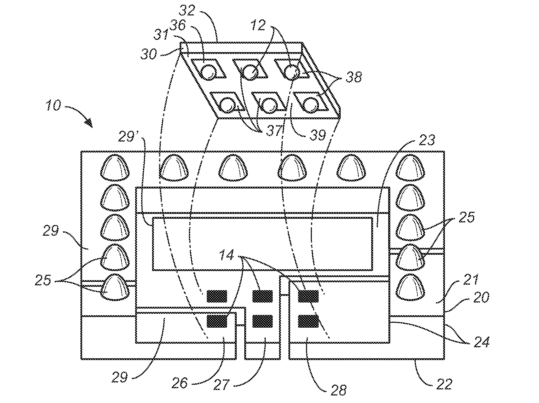
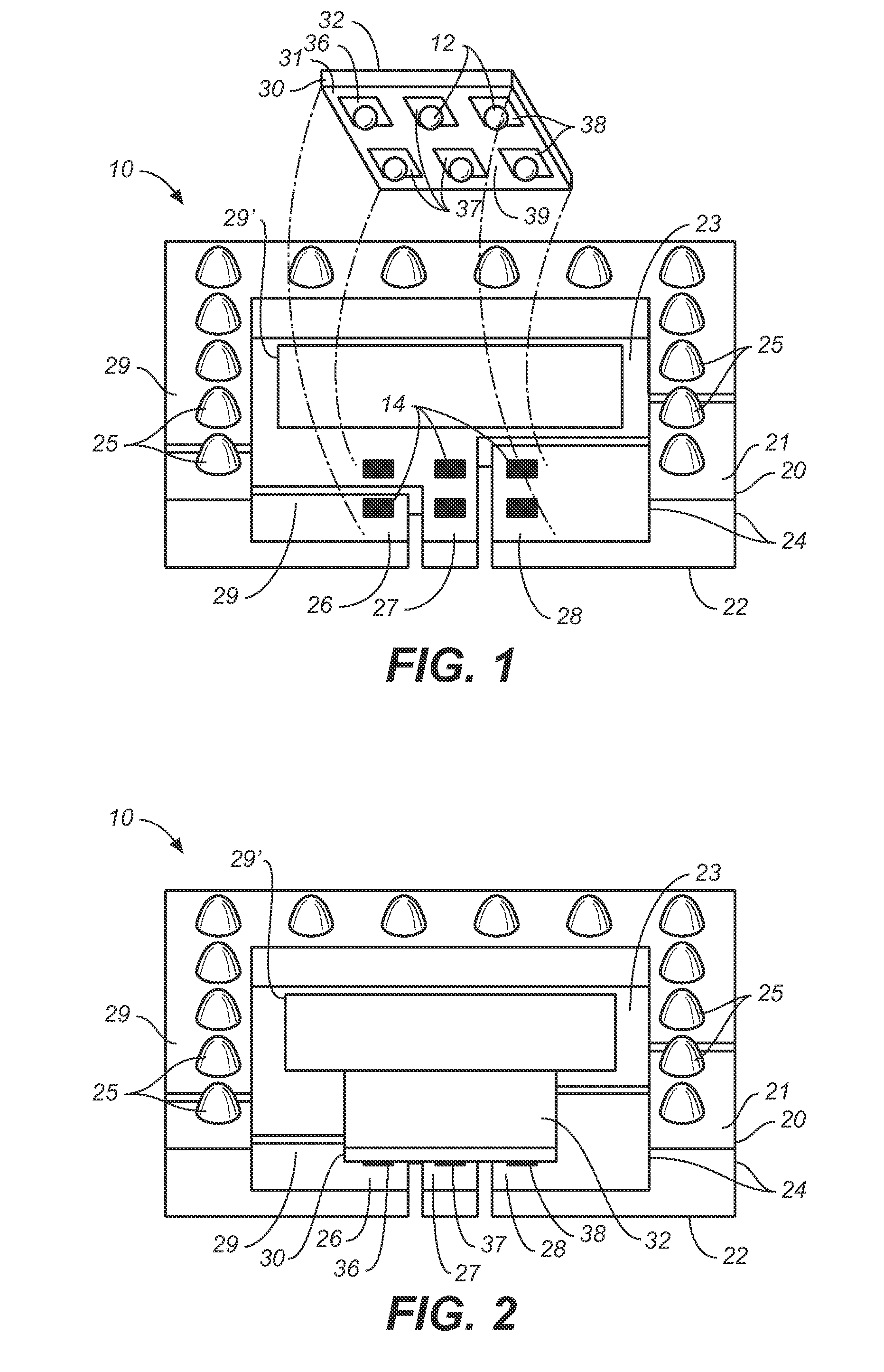
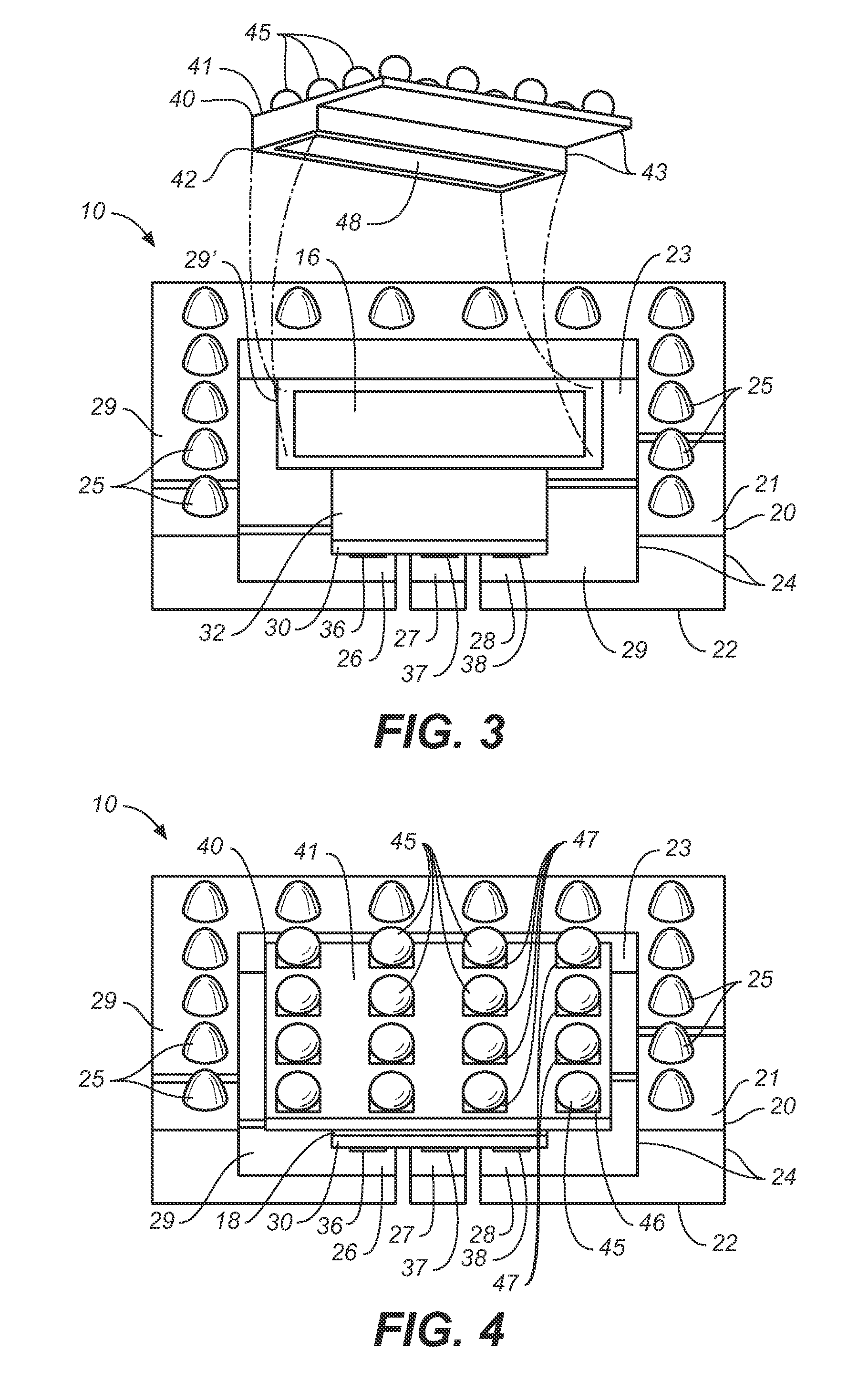
[0022]FIG. 1 shows a partial expanded perspective view of a first exemplary semiconductor die package 10 according to the present invention. Semiconductor die package 10 comprises a leadframe 20, a first semiconductor die 30, and a second semiconductor die 40 (shown in FIGS. 3 and 4). Leadframe 20 has a top surface 21, a bottom surface 22 opposite its top surface 21, a recess 23 disposed in top surface 21 to receive semiconductor dice, and a rim 24 disposed around at least a portion of recess 23. Leadframe 20 is partitioned into at least three conductive regions 26-28 (e.g., three leads). In an exemplary implementation, first semiconductor die 30 is electrically coupled to conductive regions 26-28, and second semiconductor die 40 is electrically coupled to second conductive region 27 (as illustrated in FIG. 3 and described below). A plurality of bumps 25 are disposed on rim 24 to facilitate electrical interconnections between leadframe 20 and an external substrate. There is at least...


PUM


Abstract

Disclosed are semiconductor die packages having overlapping dice, systems that use such packages, and methods of making such packages. An exemplary die package comprises a leadframe, a first semiconductor die, and a second semiconductor die that has a recessed portion in one of its surfaces. The first die is disposed over a first portion of the leadframe, and the second die is disposed over a second portion of the leadframe with its recess portion overlying at least a portion of the first die. Another exemplary die package comprises a leadframe with a recessed area, a first semiconductor die disposed in the recessed area, and a second semiconductor die overlying at least a portion of the first die. Preferably, electrically conductive regions of both dice are electrically coupled to a conductive region of the leadframe to provide an interconnection between dice that has very low parasitic capacitance and inductance.

Description

CROSS-REFERENCES TO RELATED APPLICATIONS[0001]NOT APPLICABLEBACKGROUND OF THE INVENTION[0002]Semiconductor die packages are currently used in power supplies for computers. Because these die packages dissipate large amounts of heat for these applications, one semiconductor device is generally provided in each package so as to allow for a dedicated heat sink for each device. A recent trend in the industry has been to use a system of distributed power supplies in computers, server systems, and other electronic devices and the like, where several smaller buck converters supply individual components instead of a single power converter, such as a forward converter. In the distributed buck-converter configuration, the input AC power can be converted by an AC-to-DC converter to an intermediate DC voltage that is unregulated, or lightly-regulated, typically in the range of 5 to 50 volts, and a plurality of distributed DC-to-DC buck converters convert the intermediate DC voltage to regulated ...

Claims


Application Information

Patent Timeline
IPC IPC(8): H01L23/495H01L21/60
CPCH01L23/49548H01L2924/01033H01L23/49575H01L24/13H01L24/16H01L24/29H01L24/32H01L24/73H01L24/81H01L2224/732H01L2924/01029H01L2924/01046H01L2924/01079H01L2924/01082H01L2924/13091H01L2924/19041H01L2924/19042H01L2924/30105H01L2924/30107H01L2924/01006H01L23/49562H01L2224/05571H01L2224/05573H01L2224/06131H01L2924/00014H01L2224/05599
Inventor IRVING, SCOTTLIU, YONGQIAN, QIUXIAO
Owner SEMICON COMPONENTS IND LLC
Why Eureka
Try Eureka