
Optical device comprising a charge transport layer of insoluble organic material and method for the production thereof

Active Publication Date: 2009-07-09
CAMBRIDGE DISPLAY TECH LTD
View PDF33 Cites 32 Cited by
  • Summary
  • Abstract
  • Description
  • Claims
  • Application Information

AI Technical Summary

Benefits of technology

[0021]The present inventors have surprisingly found that the charge transporting layer may be rendered insoluble in the solvent even when cross-linking groups are absent. Accordingly, in another embodiment the charge transporting layer is substantially free of cross-linkable groups and the treatment comprises subjecting the charge transporting layer to heat.
[0064]Similarly, it may be desirable to provide a charge injecting layer comprising a conductive organic material for injecting charge carriers of the first type remote from the electroluminescent layer to prevent any quenching that may occur if these layers are adjacent (e.g. quenching by a polaron band of the conductive organic material).

Problems solved by technology

However, solution deposition of multiple layers is complicated by the tendency of initially cast or deposited layers to dissolve in the solvents used for succeeding layers.
This approach is limited in that the material used for the first layer can only be selected from those that do not dissolve in the solvent used for the second layer.
Again, this approach is limited in that it is only applicable to insoluble compounds that have a soluble precursor form.
Furthermore, the thermal conversion required by these precursors requires forcing conditions and generates corrosive by-products that may harm the performance of the finished device.

Method used


Image

  • Optical device comprising a charge transport layer of insoluble organic material and method for the production thereof
  • Optical device comprising a charge transport layer of insoluble organic material and method for the production thereof
  • Optical device comprising a charge transport layer of insoluble organic material and method for the production thereof

Examples


example 1

[0131]The general procedure above was followed using an electroluminescent layer comprising:[0132]a host polymer having the composition 70% 9,9-dioctylfluorene-2,7-diyl, 10% 9,9-diphenylfluorene-2,7-diyl, 10% “TFB” repeat unit and 10% “PFB” repeat unit as disclosed in WO 02 / 92723 (TFB and PFB repeat units are illustrated below). The polymer was prepared by Suzuki polymerisation as disclosed in, for example, WO 00 / 53656.

[0133]the red phosphorescent dopant platinum octaethylporphine (PtOEP) as disclosed in Nature (London), 1998, 395, 151.

[0134]The host:dopant ratio was 98.8:1.2.

[0135]The hole transporting layer was subjected to heat treatment at 130° C. for 10 minutes prior to deposition of the electroluminescent layer.

example 2

[0137]A device was made in accordance with Example 1 except that the host:dopant ratio was 98.0:2.0.

example 3

[0139]A device was made in accordance with Example 1 except that the electroluminescent layer consisted of host material CBP and the green electroluminescent dendrimer dopant ED1, disclosed in WO 02 / 066552 and illustrated below, deposited by spin-coating from a chloroform solution having a CBP:ED1 ratio of 8:2.


PUM

PropertyMeasurementUnit
Electric chargeaaaaaaaaaa
Electrical conductoraaaaaaaaaa
Phosphorescence quantum yieldaaaaaaaaaa

Abstract

A method of forming an organic light emitting diode comprising the steps of: providing a substrate comprising a first electrode for injection of charge carriers of a first type; forming a charge transporting layer by depositing over the substrate a charge transporting material for transporting charge carriers of the first type, the charge transporting material being soluble in a solvent; treating the charge transporting layer to render it insoluble in the solvent; forming an electroluminescent layer by depositing onto the charge transporting layer a composition comprising the solvent, a phosphorescent material, and a host material; and depositing over the electroluminescent layer a second electrode for injection of charge carriers of a second type.

Description

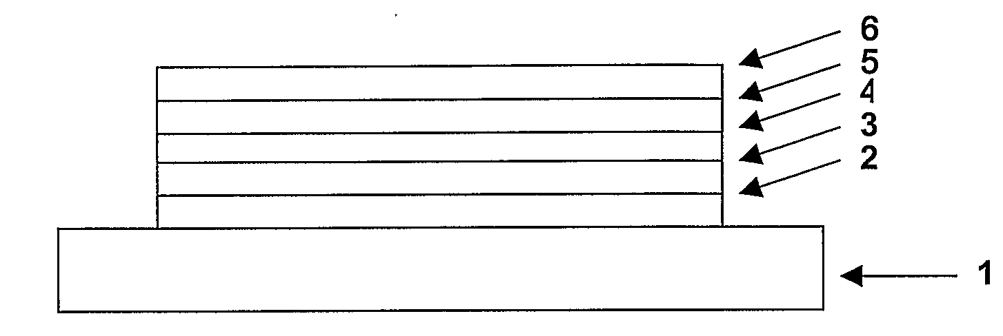
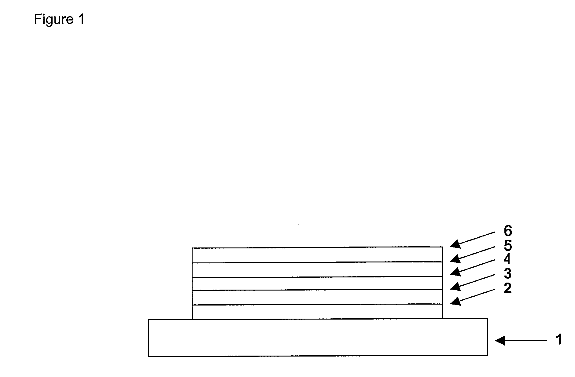
FIELD OF THE INVENTION[0001]This invention relates to organic optical devices comprising a layer of insoluble organic material and methods for the production thereof.BACKGROUND OF THE INVENTION[0002]Organic semiconductors are now frequently used in a number of optical devices such as in organic light emitting diodes (“OLEDs”) as disclosed in WO 90 / 13148, photovoltaic devices as disclosed in WO 96 / 16449 and photodetectors as disclosed in U.S. Pat. No. 5,523,555.[0003]A typical OLED comprises a substrate, on which is supported an anode (commonly indium tin oxide or “ITO”), a cathode and an organic electroluminescent layer between the anode and cathode. In operation, holes are injected into the device through the anode and electrons are injected into the device through the cathode. The holes and electrons combine in the organic electroluminescent layer to form an exciton which then undergoes radiative decay to give light. Other layers may be present in the OLED, for example a layer of ...

Claims


Application Information

Patent Timeline
IPC IPC(8): H01J1/63H01L51/56H01L51/00H01L51/30H01L51/40H01L51/50H05B33/14
CPCH01L51/0003H01L51/0037H01L51/0039H01L51/0043H01L51/0059Y10S428/917H01L51/0084H01L51/0085H01L51/5016H01L51/5048H01L51/56H01L51/0062H10K71/12H10K85/1135H10K85/115H10K85/151H10K85/649H10K85/631H10K85/341H10K85/342H10K50/14H10K50/11H10K2101/10H10K71/00H10K50/155H10K50/17H10K50/18H10K50/81H10K50/82H10K50/121H10K85/6572
Inventor PATEL, NALINKUMAR L.CONWAY, NATASHA M.LEADBEATER, MARKGRIZZI, ILARIA
Owner CAMBRIDGE DISPLAY TECH LTD
Learn More