Charged Particle Beam Device With Retarding Field Analyzer

a charger and charger technology, applied in the direction of material analysis using wave/particle radiation, instruments, separation processes, etc., can solve the problems of affecting the primary charge particle beam, the field of the charger will also disturb the charger beam, and the small stray field region ratio is difficult to achieve. , to achieve the effect of high spatial resolution, high energy resolution and high spatial resolution

Active Publication Date: 2009-08-13
ICT INTEGRATED CIRCUIT TESTING GESELLSCHAFT FUER HALBLEITERPRUEFTECHNIK GMBH
View PDF11 Cites 48 Cited by
  • Summary
  • Abstract
  • Description
  • Claims
  • Application Information

AI Technical Summary

Benefits of technology

[0028]The charged particle beam device according to the invention is capable of inspecting a specimen with high spatial resolution and high throughput by means of an energy dependent detection of secondary charged particles. The at least one further electrode element, the at least one ring electrode and / or the at least one high-ohmic electrode make it possible to electrically shield the secondary charged particles from the beam tube element. Further, they can be used to reduce the size of stray field regions within the retarding electric field region, which improves the energy resolution for the detection of the secondary charged particles. A high energy resolution is important for voltage or material contrast measurements on a specimen, where an energy resolution of the secondary charged particles within the eV range and better is needed.
[0079]Preferably, the tube voltage VT differs by more than +4000 V and even more preferred by more than +8000 V from the first voltage V1. This allows the tube voltage VT to be operated at a high voltage with respect to the voltage of the specimen. In principal, the higher the tube voltage VT relative to the voltage of the specimen, the more precise the focussing of the primary charged particles beam and the higher the spatial resolution of the measurements.

Problems solved by technology

However, problems arise when the entrance grid electrode and the filter grid electrode are not coplanar or not concentric.
However, providing a small stray field region ratio is difficult to achieve if the space for the retarding electric field region within the charged particle beam device is small.
However, it is difficult to design a retarding field analyzer with a small stray field region if the retarding field analyzer is placed near or within the high voltage beam tube, since the high voltage intrudes into the retarding electric field and increases the stray field region.
Vice versa, the electric fields of the retarding field analyzer will also disturb the primary charged particle beam in regions where the charged particle beam is not shielded.
Therefore, it represents a considerable problem for the retarding field analyzer to discriminate secondary charged particles within an energy range of a few eV or less while the mean energy of the secondary charged particles is in the range of several keV.

Method used


Image

  • Charged Particle Beam Device With Retarding Field Analyzer
  • Charged Particle Beam Device With Retarding Field Analyzer
  • Charged Particle Beam Device With Retarding Field Analyzer

Examples


Embodiment Construction

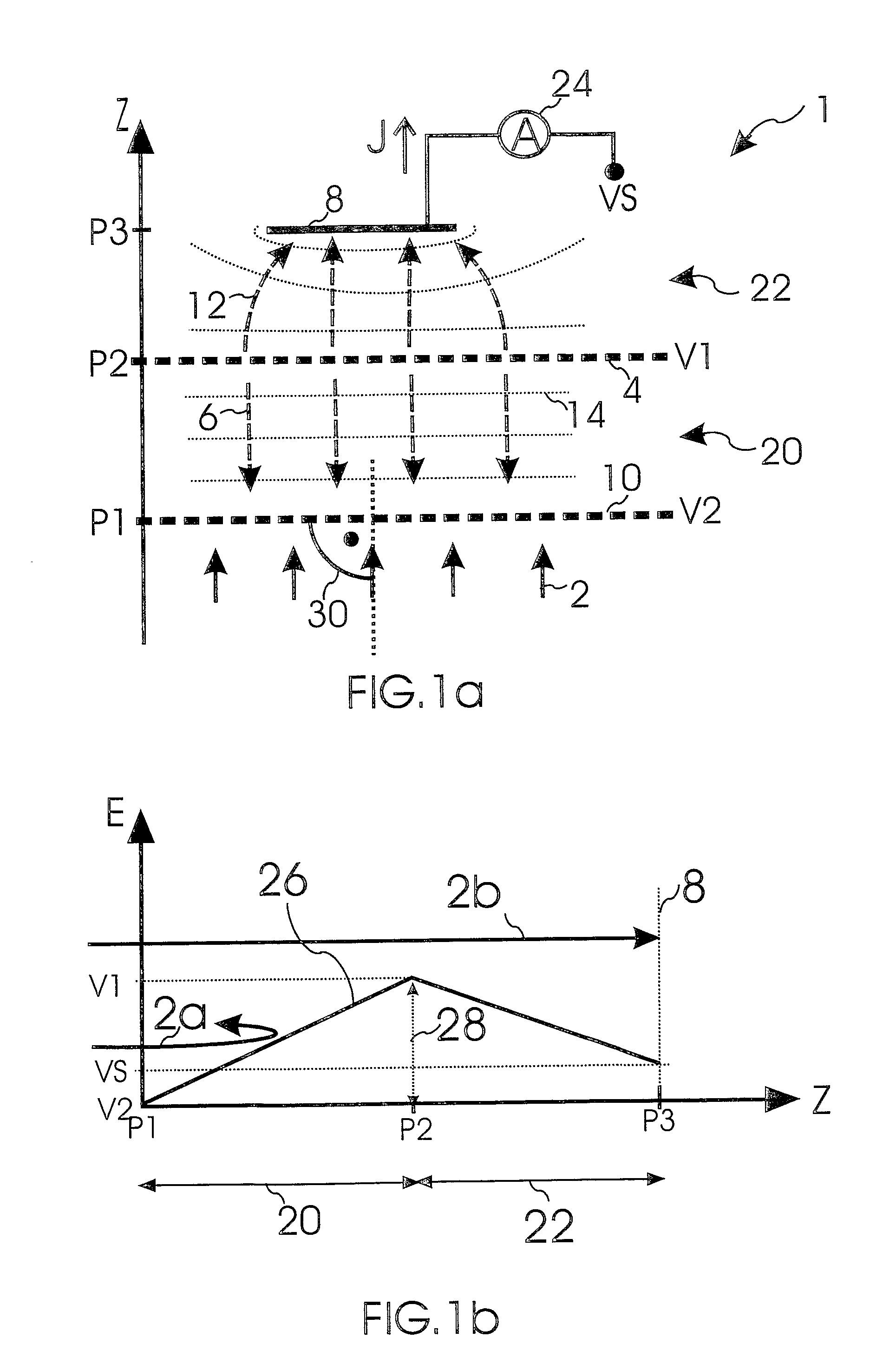
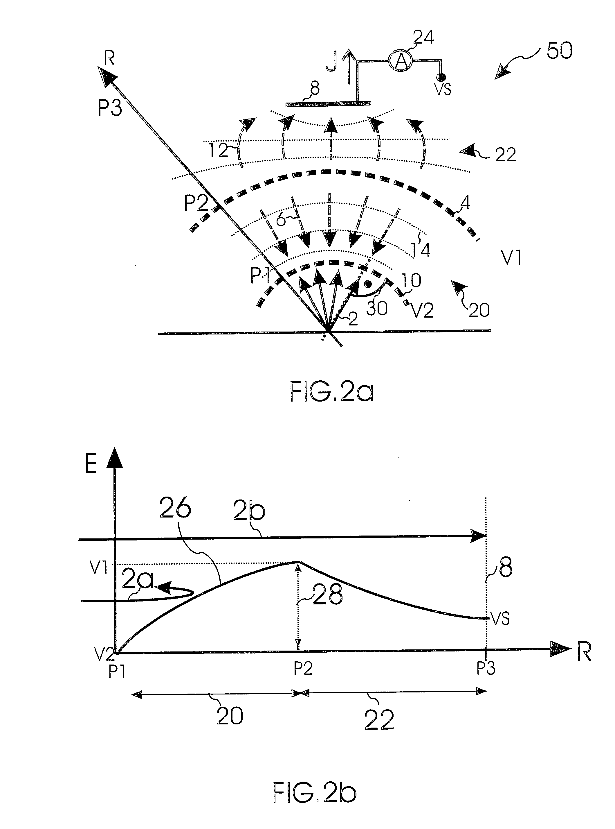
[0105]FIGS. 1 to 4 have already been described in detail in the introduction of the application.

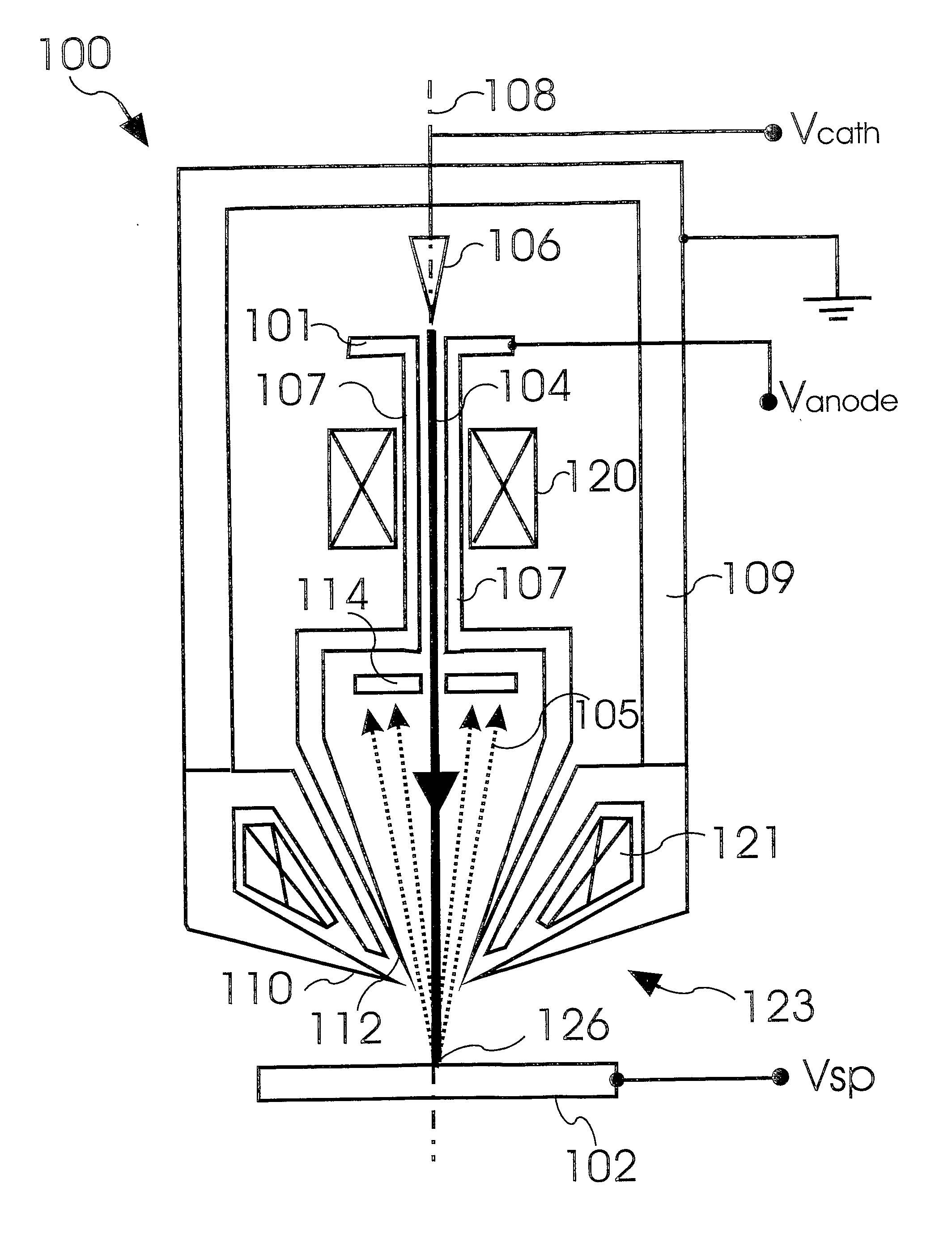
[0106]FIG. 5 shows a cross section of a first embodiment of a charged particle beam device according to the invention, i.e. a cross section of an electron beam microscope 100. The electron beam microscope 100 like the one shown in FIG. 4 comprises a high voltage beam tube 107 and a combined electrostatic magnetic focus lens 123. However, in this embodiment, an in-lens planar retarding field analyzer 1 is used to discriminate the incoming secondary charged particles 105 according to their energy. For an electron beam device, the term “secondary charged particles” refers equally to secondary electrons (energy smaller than 50 eV, by definition) and backscattered electrons (energy larger than 50 eV, by definition).

[0107]The high energy resolution capabilities of a retarding field analyzer 1 allow different energy distributions of the incoming secondary charged particles 105 to be distinguishe...


PUM

PropertyMeasurementUnit
voltageaaaaaaaaaa
voltageaaaaaaaaaa
currentaaaaaaaaaa

Abstract

The invention provides a charged particle beam device to inspect or structure a specimen with a primary charged particle beam propagating along an optical axis; a beam tube element having a tube voltage; and a retarding field analyzer in the vicinity of the beam tube element to detect secondary charged particles generated by the primary charged particle beam on the specimen. According to the invention, the retarding field analyzer thereby comprises an entrance grid electrode at a second voltage; at least one filter grid electrode at a first voltage; a charged particle detector to detect the secondary charged particles; and at least one further electrode element arranged between the entrance grid electrode and the at least one filter grid electrode. The at least one further electrode element reduces the size of the stray fields regions in the retarding electric field region to improve the energy resolution of the retarding field analyzer. The improvement of the energy resolution is significant, in particular when the beam tube element is part of a high voltage beam tube.

Description

BACKGROUND OF THE INVENTION[0001]1. Field of the Invention[0002]The invention relates to a charged particle beam device using a retarding field analyzer to inspect specimens with a primary charged particle beam. The invention also relates to a retarding field analyzer that can be used in devices like a charged particle beam device.[0003]2. Description of the Related Art[0004]Retarding field analyzers in charged particle beam devices are frequently used to analyze the energy distributions of secondary charged particles that are generated by a primary charged particle beam on a specimen. Since the energy distributions of the secondary charged particles carry information about the electrical potential and material of the specimen in the region where the primary charged particle beam interacts with the specimen, a scanning charged particle beam device with a retarding field analyzer can be used to generate a map with voltage or material distributions on the surface of the specimen. Such...

Claims


Application Information

Patent Timeline
Patent Type & Authority Applications(United States)
IPC IPC(8): G01N23/00H01J47/00G01R31/305G01R31/307H01J37/244H01J37/28
CPCG01R31/305H01J2237/24585H01J2237/24485H01J37/244
Inventor DEGENHARDT, RALFFEUERBAUM, HANS-PETERHAMBACH, DIRKKOGLER, WALTERMUNACK, HARRYSALVESEN, CARLO
Owner ICT INTEGRATED CIRCUIT TESTING GESELLSCHAFT FUER HALBLEITERPRUEFTECHNIK GMBH
Why Eureka
Try Eureka