Semiconductor device manufacturing method, wiring and semiconductor device
a semiconductor device and manufacturing method technology, applied in the direction of semiconductor devices, basic electric elements, electrical appliances, etc., can solve the problems of inability to uniformly form the silicide layer, the increase of the operating speed of the smaller elements cannot be expected, and the various problems relating to the silicide layer formed by the process aris
- Summary
- Abstract
- Description
- Claims
- Application Information
AI Technical Summary
Benefits of technology
Problems solved by technology
Method used
Image

Examples
embodiment 1
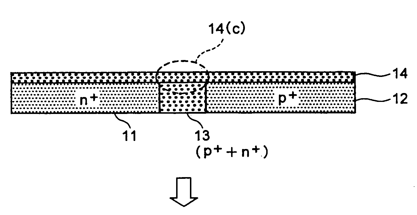
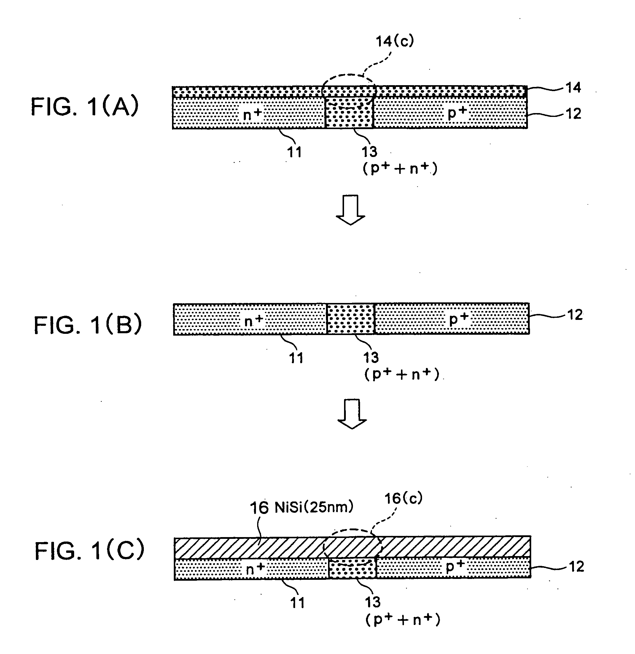
[0049]FIGS. 1(A), 1(B), and 1(C) are schematic sectional views for explaining the structure of a semiconductor device and a method of manufacturing the semiconductor device in Embodiment 1 of the present invention.
[0050]FIGS. 1(A), 1(B), and 1(C) show only extracted portions: a polycrystalline silicon gate electrode and a wiring portion, for ease of explanation, omitting processes of forming a device separation region, a source, a drain, a well, a channel, and a gate side wall spacer, necessary for manufacture of an actual transistor. Also, gate oxide film is not shown in the figures.
[0051]As shown in FIG. 1(A), an impurity segregation layer 14 where the impurities segregate at a high concentration is formed to a thickness of about 5 nm by performing RTA as an activating heat treatment at 1000° C. or more for 10 seconds or less on surface layers in the n+ polycrystalline silicon region 11 and the p+ polycrystalline silicon region 12.
[0052]The boundary region 13 adjacent to the n+ po...
embodiment 2
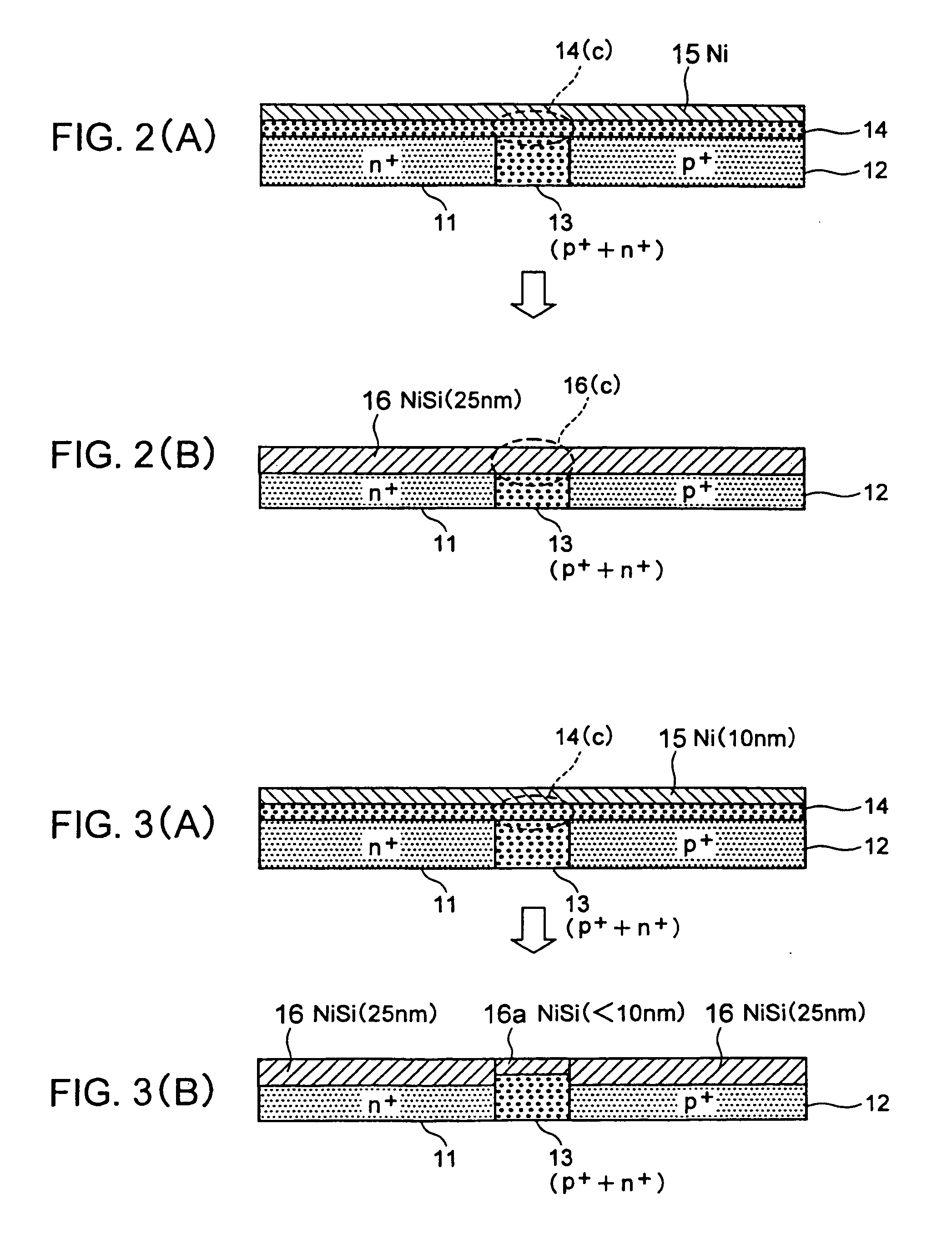
[0059]FIGS. 2(A) and 2(B) are schematic sectional views for explaining the structure of a semiconductor device and a method of manufacturing the semiconductor device in Embodiment 2 of the present invention.
[0060]FIGS. 2(A) and 2(B) show only extracted portions: a polycrystalline silicon gate electrode and a wiring portion, for ease of explanation, omitting processes of forming a device separation region, a source, a drain, a well, a channel, and a gate side wall spacer, necessary for manufacture of an actual transistor, as do FIGS. 1(A) to 1(C). Also, gate oxide film is not shown in the figures.
[0061]As shown in FIG. 2(A), an impurity segregation layer 14 where the impurities segregate at a high concentration is formed by performing RTA as an activating heat treatment at 1000° C. or more for 0 to 10 seconds on surface layers in the n+ polycrystalline silicon region 11 and the p+ polycrystalline silicon region 12.
[0062]The boundary region 13 adjacent to the n+ polycrystalline silico...
PUM
| Property | Measurement | Unit |
|---|---|---|
| temperature | aaaaa | aaaaa |
| thickness | aaaaa | aaaaa |
| depth | aaaaa | aaaaa |
Abstract
Description
Claims
Application Information