Organic Electro-Luminescence Device

a technology of electroluminescence device and organic material, which is applied in the direction of discharge tube/lamp details, discharge tube luminescnet screen, organic semiconductor device, etc., can solve the problems of poor electron injection efficiency of organic electroluminescence device, sputtering process of ito material, and affecting the efficiency of light utilization, etc., to achieve high electron injection efficiency

Active Publication Date: 2009-08-20
AU OPTRONICS CORP
View PDF15 Cites 2 Cited by
  • Summary
  • Abstract
  • Description
  • Claims
  • Application Information

AI Technical Summary

Benefits of technology

[0014]It is an object of the present invention to provide an organic electro-luminescence device with high electron injection efficiency.
[0015]It is another object of the present invention to solve the prior disadvantage of decreased life time of organic materials.
[0016]It is another object of the present invention to provide a method for fabricating an organic electro-luminescence device without complicated process.

Problems solved by technology

Said wires or TFTs would restrict the light utilizing efficiency because of a limited aperture ratio.
While applying conductive transparent material like ITO for the electron injection layer 150, a major issue is that sputtering process of the ITO material would damage the organic materials (140) beneath.
However, while practical estimated, the electron injection efficiency of the organic electro-luminescence device 100a is too poor to apply in commercial application.
This may decrease the life time of the organic electro-luminescence device.
The complicated process (at least three times of movement between different chambers) is a disadvantage of organic electro-luminescence device 100b.

Method used


Image

  • Organic Electro-Luminescence Device
  • Organic Electro-Luminescence Device
  • Organic Electro-Luminescence Device

Examples


Embodiment Construction

[0024]The invention aims at providing an organic electro-luminescence devices and particularly to a top-emission organic electro-luminescence device, which has high current injection efficiency, relatively loner life time, and can be fabricated with relatively simplified processes.

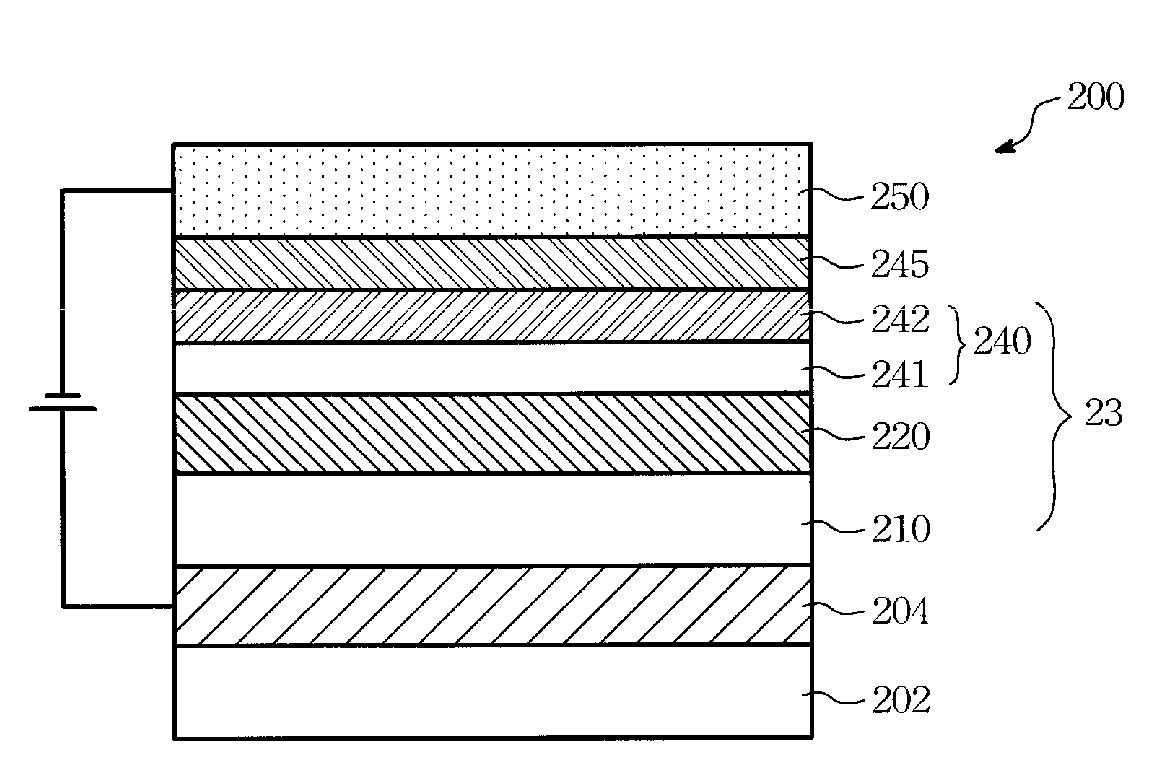
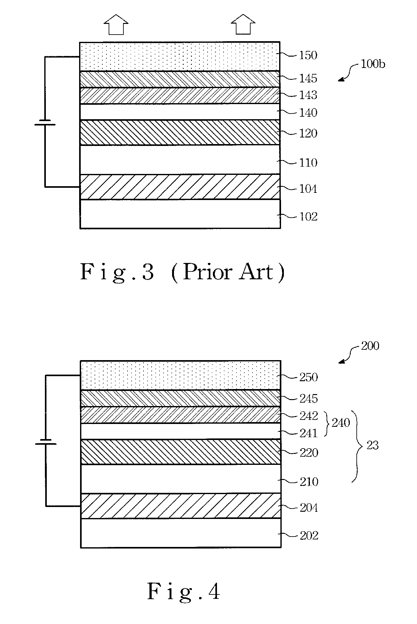
[0025]Please refer to FIG. 4, which is a cross section view of an organic electro-luminescence device of the present invention. While fabricating the organic electro-luminescence device 200, a substrate 202 is provided first, then a hole injection layer 204 is disposed on the substrate 202. In one embodiment, the substrate 202 is made of light transparent materials or opaque materials with light reflection character. The hole injection layer 204 is made of conductive transparent materials (for instance, ITO, IZO) via sputtering process.

[0026]Next, an organic layer 23 is disposed on the hole injection layer 204. Wherein the organic layer 23 is an multi-layer structure. It at least comprises a light-emitting...


PUM

PropertyMeasurementUnit
brightnessaaaaaaaaaa
life timeaaaaaaaaaa
organicaaaaaaaaaa

Abstract

A method of fabricating an organic electro-luminescence device comprising the steps of providing a substrate, an organic chamber, and a sputtering chamber, forming a hole injection layer on the substrate, forming a hole transport layer on the hole injection layer in the organic chamber, forming a light-emitting layer on the hole transport layer in the organic chamber, disposing a metal chelate material on the light-emitting layer and partially doping a CsF compound into the metal chelate material to forming an electron transporting layer in the organic chamber, forming a buffer layer on the electron transporting layer in the organic chamber, transferring the substrate, the hole injection layer, the hole transport layer, light-emitting layer, the electron transporting layer, and the buffer layer form the organic chamber to the sputtering chamber, and forming an electron injection layer on the buffer layer in the sputtering chamber

Description

CROSS-REFERENCE TO RELATED APPLICATIONS[0001]This application is a continuation of U.S. patent application Ser. No. 11 / 315,172, filed Dec. 23, 2005.BACKGROUND OF THE INVENTION[0002](1) Field of the Invention[0003]The present invention relates generally to organic electro-luminescence devices (OLEDs) and particularly to a top-emission organic electro-luminescence device.[0004](2) Description of the Prior Art[0005]Organic electro-luminescence devices become popular in display technology these days. Comparing to another popular display—liquid crystal display (LCD), the organic electro-luminescence devices have the advantage of self light-emitting. Hence, backlight module is no more needed in a panel display applied OLEDs.[0006]Please refer to FIG. 1, which is a cross-section view of the structure of an organic electro-luminescence device. The electro-luminescence device 100 comprises, in the sequence from bottom to top, a substrate 102, a hole injection layer 104, a hole transport laye...

Claims


Application Information

Patent Timeline
Patent Type & Authority Applications(United States)
IPC IPC(8): H01J1/63C23C14/34
CPCC09K11/06C09K2211/186H01L51/0059H01L51/0078H05B33/14H01L51/5052H01L51/5092H01L51/5234H01L2251/5315H01L51/0081H10K85/311H10K85/631H10K85/324H10K50/165H10K50/171H10K50/828H10K2102/3026
Inventor LI, SHI-HAOIOU, CHUNG-YEH
Owner AU OPTRONICS CORP
Why Eureka
Try Eureka