Display panel and method for manufacturing the same

a technology of display panel and manufacturing method, which is applied in the field of display panel, can solve the problems of poor adhesion characteristic, difficult to reliably execute thickening of signal lines, and reduced reliability of low resistance metal adapted to the actual process, so as to reduce the thickness of signal lines, prevent lifting and peeling of signal lines, and reduce the resistance of signal lines

Inactive Publication Date: 2009-08-27
SHENZHEN CHINA STAR OPTOELECTRONICS TECH CO LTD
View PDF6 Cites 19 Cited by
  • Summary
  • Abstract
  • Description
  • Claims
  • Application Information

AI Technical Summary

Benefits of technology

[0031]According to an exemplary embodiment of the present invention, the gate line and the data line are formed with a double-layered structure such that adhesion with the substrate or the lower layer may be improved and lifting and peeling of the signal lines as well as signal delay may be simultaneously prevented.
[0032]Also, the gate line and data line are thickly formed such that the resistance of the signal lines may be reduced, and the upper gate line and the upper data line are not overlapped such that the entire thickness of the signal lines is decreased, and as a result an increase of the load of the substrate is prevented to thereby prevent the substrate from bending.
[0033

Problems solved by technology

For a signal line with low resistance, a method in which a low resistance metal such as aluminum (Al), copper (Cu), and silver (Ag) is deposited and patterned by photolithography has been proposed, but the low resistance metal has a poor adhesion characteristic with a glass substrate and may be diffused into a lower layer or an upper layer such that the reliability when the low resistance metal is ad

Method used


Image

  • Display panel and method for manufacturing the same
  • Display panel and method for manufacturing the same
  • Display panel and method for manufacturing the same

Examples


exemplary embodiment 1

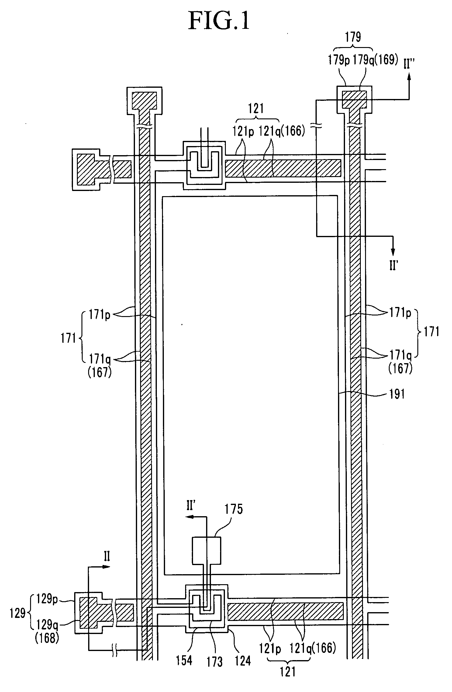
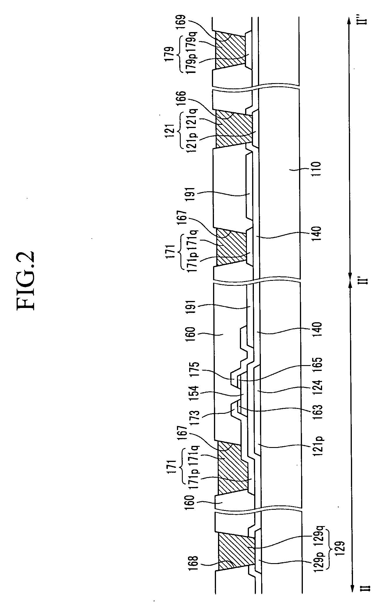
[0055]Firstly, an exemplary embodiment of a thin film transistor array panel according to the present invention will be described with reference to FIG. 1 and FIG. 2.

[0056]FIG. 1 is a top plan layout view of an exemplary embodiment of a thin film transistor array panel according to the present invention, and FIG. 2 is a cross-sectional view of the exemplary embodiment of a thin film transistor array panel shown in FIG. 1 taken along line II-II′-II″.

[0057]A plurality of lower gate lines 121p are formed on an insulating substrate 110, exemplary embodiments of which may be made of transparent glass, plastic or other materials with similar characteristics. The lower gate lines 121p extend in a substantially horizontal direction, and each lower gate line 121p includes a plurality of gate electrodes 124 projecting outward from the lower gate line 121p with a wide width, and an end portion 129p having a large area for contact with an external driving circuit. Alternative exemplary embodime...

exemplary embodiment 2

[0093]Now, another exemplary embodiment of the present invention will be described in detail with reference to FIG. 13 and FIG. 1.

[0094]FIG. 13 is a cross-sectional view of another exemplary embodiment of a TFT array panel according to the present invention. Like descriptions between the exemplary embodiments will be mainly omitted, and like reference numerals will be used for like elements.

[0095]The present exemplary embodiment is substantially the same as the above exemplary embodiment in many respects, and therefore only that which is different from the previous exemplary embodiment will be thoroughly described.

[0096]A lower gate line 121p including gate electrodes 124 and an end portion 129p is formed on an insulation substrate 110, and a gate insulating layer 140, a semiconductor island 154, and ohmic contacts 163 and 165 are formed thereon. A pixel electrode 191 is formed on the gate insulating layer 140, and a lower data line 171p including source electrodes 173 and an end po...

exemplary embodiment 3

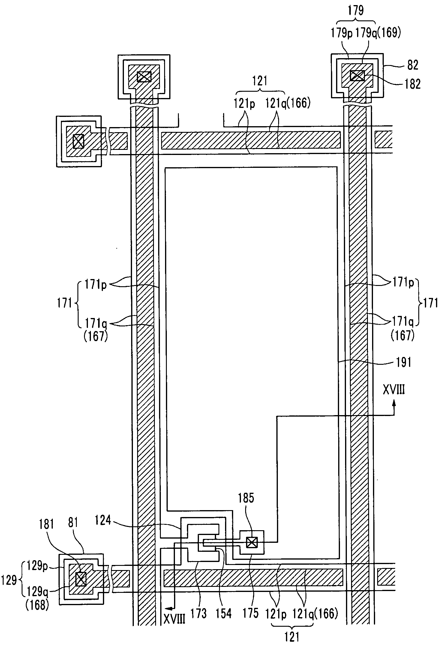
[0106]Next, another exemplary embodiment according to the present invention will be described with reference to FIG. 17 and FIG. 18.

[0107]FIG. 17 is a top plan layout view of another exemplary embodiment of a TFT array panel according to the present invention, and FIG. 18 is a cross-sectional view of the exemplary embodiment of a TFT array panel shown in FIG. 17 taken along line XVIII-XVIII.

[0108]Like descriptions between the exemplary embodiments will be mainly omitted, and like reference numerals will be used for like elements.

[0109]A plurality of lower gate lines 121p are formed on an insulation substrate 110. The lower gate line 121p includes a wiring portion mainly extending in the substantially horizontal direction, a gate electrode 124 extending upward from the wiring portion, and an end portion 129p disposed on the end of the wiring portion and having a wide width for connection with an external circuit.

[0110]A gate insulating layer 140 is formed on the lower gate line 121p ...


PUM


Abstract

A display panel includes; a lower gate line, a lower data line disposed substantially perpendicular to the lower gate line, a thin film transistor (“TFT”) connected to the lower gate line and the lower data line, an insulating layer disposed on the lower gate line, the lower data line, and the TFT and having a plurality of trenches exposing the lower gate line and the lower data line, an upper gate line disposed in the trench on the lower gate line, an upper data line disposed in the trench on the lower data line, and a pixel electrode connected to the TFT.

Description

[0001]This application claims priority to Korean Patent Application No. 10-2008-0015881 filed on Feb. 21, 2008 and all the benefits accruing therefrom under 35 U.S.C. §119, the contents of which in its entirety are herein incorporated by reference.BACKGROUND OF THE INVENTION[0002](a) Field of the Invention[0003]The present invention relates to a display panel and a manufacturing method thereof.[0004](b) Description of the Related Art[0005]A liquid crystal display (“LCD”), a plasma display panel (“PDP”) and an organic light emitting device (“OLED”) are among widely used flat panel displays.[0006]These display devices include at least one display panel, and the display panel includes switching elements connected to field generating electrodes and a plurality of signal lines such as gate lines and data lines to apply the voltages to the field generating electrodes by controlling the switching elements. To reduce an afterimage of the display device and to improve the resolution, the res...

Claims


Application Information

Patent Timeline
IPC IPC(8): H01L27/088H01L21/77
CPCH01L29/458H01L27/124H01L33/0041G02F1/136
Inventor YOUN, JOO-AEBAE, YANG-HOJEONG, CHANG-OHCHAI, CHONG-CHULYUN, PIL-SANGNING, HONGLONGKIM, BYEONG-BEOM
Owner SHENZHEN CHINA STAR OPTOELECTRONICS TECH CO LTD
Why Eureka
Try Eureka