

Microlithography exposure apparatus using polarized light and microlithography projection system having concave primary and secondary mirrors
a microlithography and projection system technology, applied in the field of projection exposure apparatus, can solve the problems of high incidence angle, and achieve the effect of convenient mounting, easy replacement, and convenient mounting
- Summary
- Abstract
- Description
- Claims
- Application Information
AI Technical Summary
Benefits of technology
Problems solved by technology
Method used
Image

Examples
first embodiment
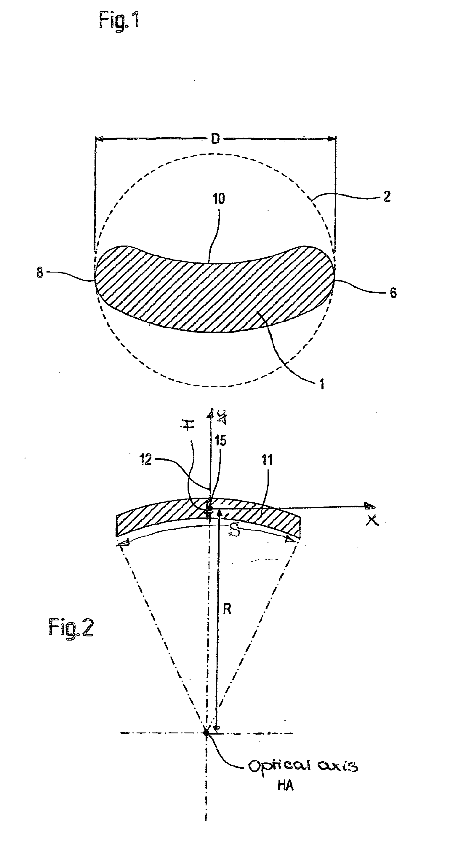
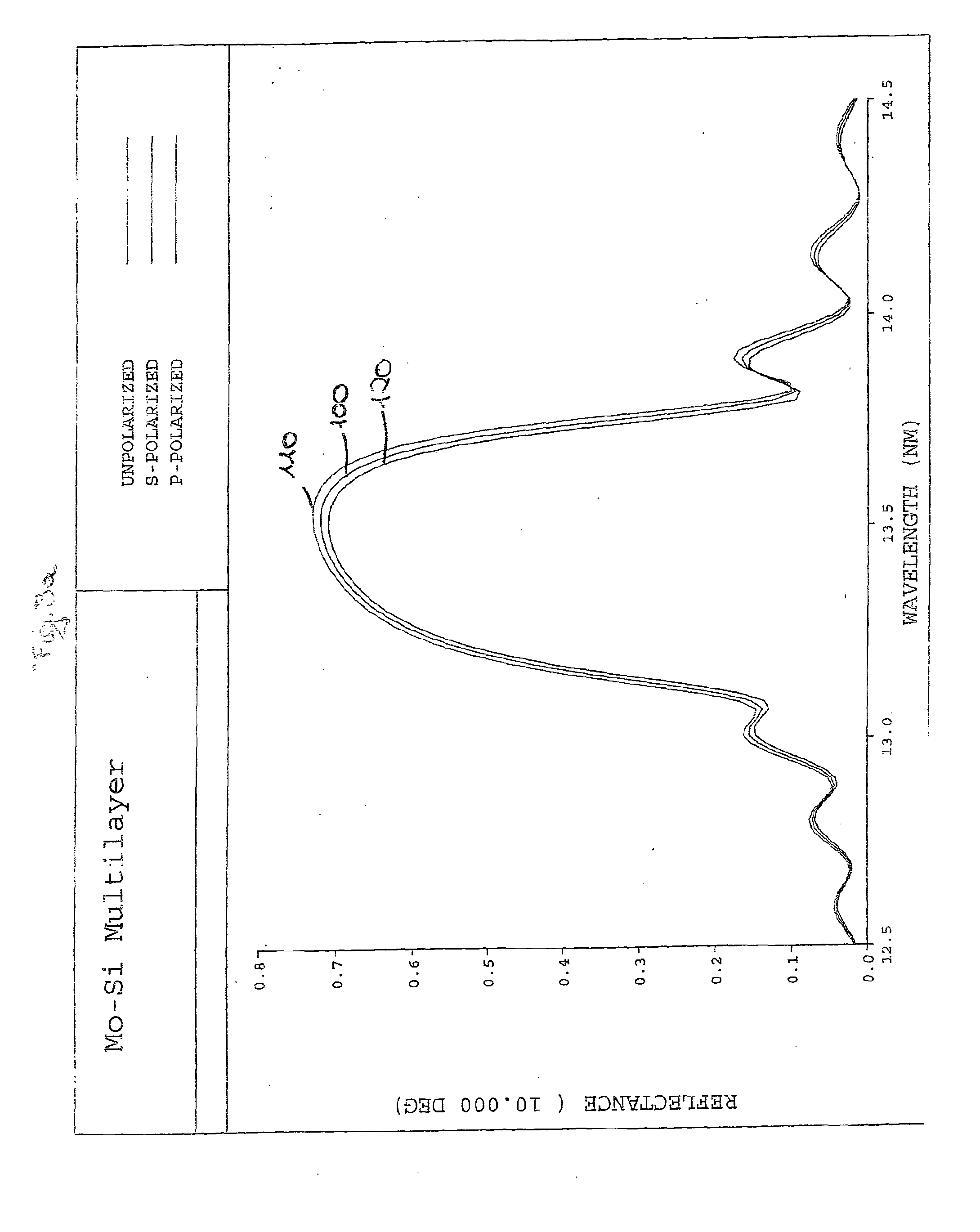
[0073]Light having the used or operation wavelength of 13.5 nm, for example, is provided by the illumination system. The essentially s-polarized light may be generated in principle in two ways in the illumination system. In the present invention, the illumination system comprises a light source which already emits s-polarized light, such as a synchotron radiation source. In an alternative embodiment, the illumination system comprises a light source which emits unpolarized light. The light is polarized within the illumination system with the aid of a polarizer, so that the reticle in the object plane is illuminated essentially with s-polarized light, for example.
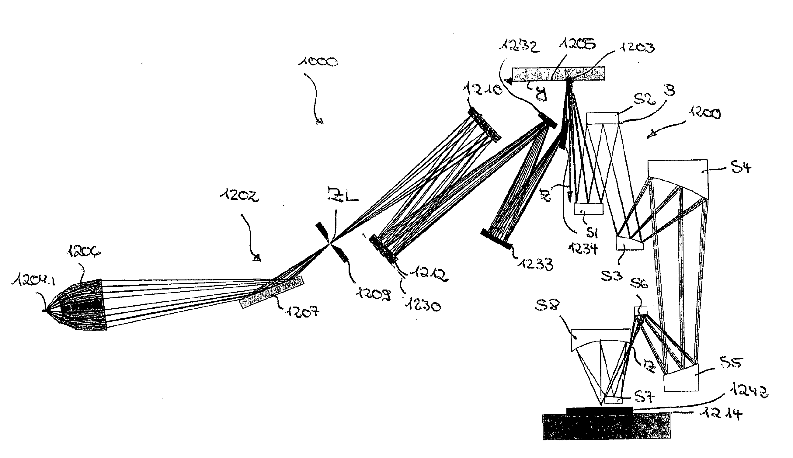
[0074]In the following FIGS. 4a.1, 4a.2, 4b, 5a, 5b, 6a, 6b, three exemplary embodiments of microlithography projection systems according to the present invention are shown. The embodiments comprising eight mirrors and have an unobscured exit pupil. In the embodiments shown in FIG. 4a.1, 4a.2, 4b, 5a, 5b, 6a, 6b the first mir...
exemplary embodiment 1
[0076 identifies the embodiment of a 8-mirror objective illustrated in FIGS. 4a. 1, 4a.2 and 4b, exemplary embodiment 2 identifies the embodiment illustrated in FIGS. 5a and 5b, and exemplary embodiment 3 identifies the embodiment illustrated in FIGS. 6a and 6b.
[0077]The wavelengths and the numerical aperture in the image plane, the field size in the image plane, the maximum field radius in the image plane, the wavefront error, the distortion, and the chief ray angle at the object, i.e., the reticle at the central field point, are specified in Table 1.
[0078]The first exemplary embodiment comprises, as shown in FIG. 4a.1, 4a.2, an object plane 300. An object in the object plane 300 is imaged with the aid of the projection system according to the present invention in the image plane 400. Proceeding from the object, a light bundle passes through the microlithography projection system from the object plane 300 to the image plane 400. The chief ray angle at the Object is denoted with y....
PUM
 Abstract
Description
Claims
Application Information