
Plating processing method, light-transmitting conductive film and electromagnetic wave-shielding film

a technology of electromagnetic shielding film and plating processing method, which is applied in the direction of magnetic/electric field screening, printed circuit manufacturing, electric discharge tubes, etc., can solve the problem that the plating cannot be directly applied to the film, and achieve the effect of effective uniform application, high productivity and uniform plating

Inactive Publication Date: 2009-09-03
FUJIFILM CORP
View PDF7 Cites 18 Cited by
  • Summary
  • Abstract
  • Description
  • Claims
  • Application Information

AI Technical Summary

Benefits of technology

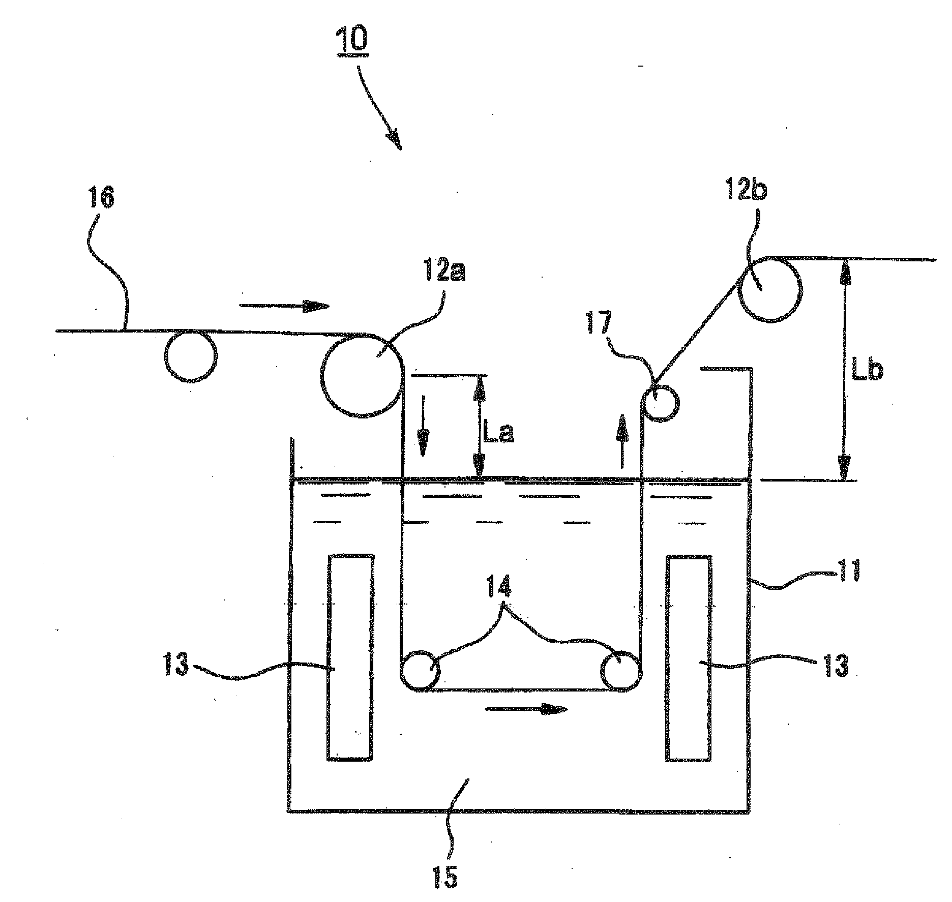
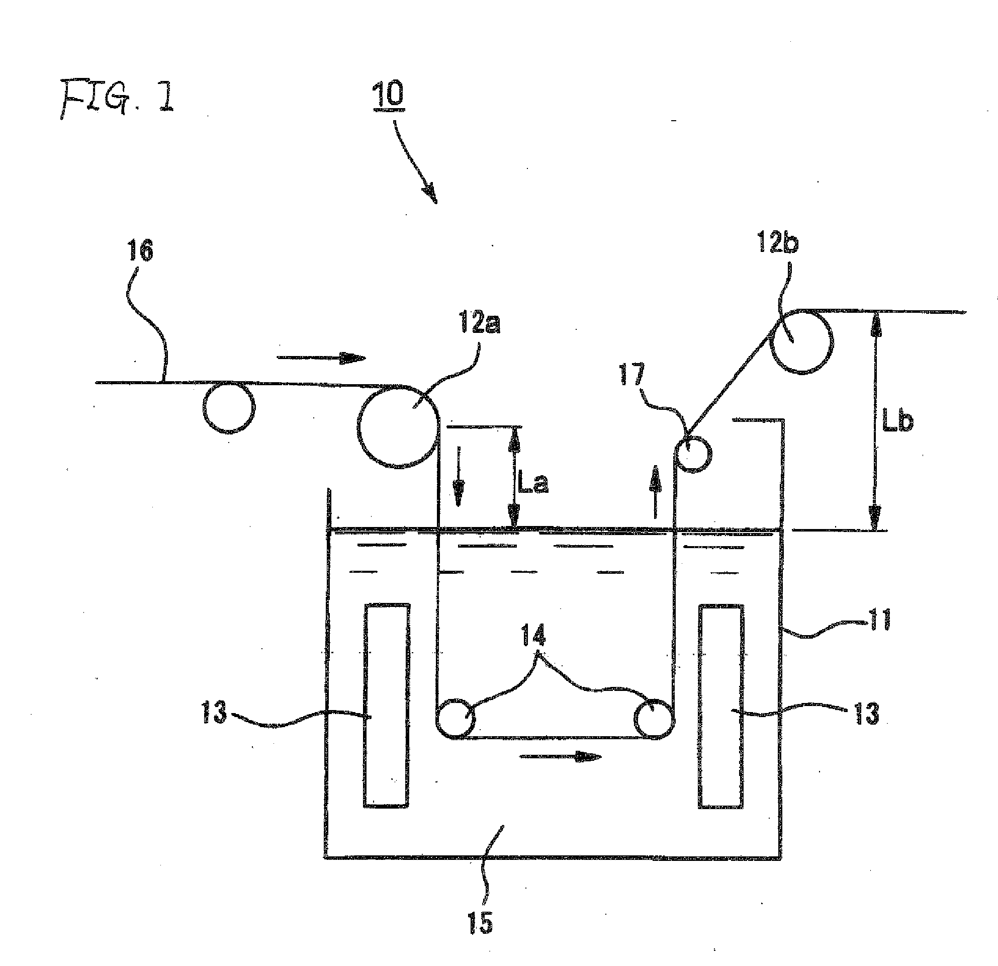
[0025]According to the plating processing method of the present invention, plating can be effectively uniformly applied to the front of a film only by electroplating. Thus, can be provided a light-transmitting conductive film and a light-transmitting electromagnetic wave-shielding film, each having uniform plating thereon at a high productivity.

Problems solved by technology

However, since a direct electroplating on an insulator film having a large surface resistivity cannot be effected, it is currently conducted that a thin metallic film is formed on an insulator film according to spattering method, vacuum deposition method or electroless plating method, thereafter electroplating is effected thereon to increase the thickness to a desired level.
However, in this film, a developed silver mesh has a high resistance and, therefore, an electroplating cannot be directly applied to the film.

Method used


Image

  • Plating processing method, light-transmitting conductive film and electromagnetic wave-shielding film
  • Plating processing method, light-transmitting conductive film and electromagnetic wave-shielding film

Examples


example 1

Silver Halide Photosensitive Material

[0250]Was prepared an emulsion containing silver iodobromochloride particles (I=0.2 mol %, Br=40 mol %) having an average particle size in terms of sphere diameter of 0.1 μm and 10.0 g of gelatin based on 60 g of Ag in an aqueous medium. K3Rh2Br9 and K2IrCl6 were added to the emulsion prepared so as to give the concentration of 10−7 (mol / mol silver) whereby Ah ion and Ir ion were doped to silver bromide particles. Further, Na2PdCl4 was added thereto, followed by effecting gold-sulfur sensitization using chloroaulic acid and sodium thiosulfate. Thereafter, the resulting product was coated on a support comprising polyethylene terephthalate (PET) together with a gelatin film hardener so that the coated amount of silver may be 1 g / m2. In this case, the volume ratio of Ag / gelatin was 1 / 2 and the thickness of PET support was 75 μm.

[0251]A coating was effected at the width of 25 cm and the length of 20 m on the PET support having the width of 30 cm and ...

example 2

[0270]A sample obtained by copper-sputtering was applied to the same PET film as that of Example 1 to reduce the surface resistivity to 50Ω / square was used instead of the photosensitive material in Example 1 and the same experiment as in Example 1 was effected. As a result, under the conditions of sample No. 3, the surface hardness of the sample was 1.5Ω / square and, therefore, it could be seen that the embodiment of Example 1 (silver mesh) was preferable.

example 3

[0271]The same plating processing was effected as in Example 1 except for preparing a sample having a width of 67 cm in place of 24 cm width. As a result, a similar result to that of Example 1 was obtained.


PUM

PropertyMeasurementUnit
surface resistivityaaaaaaaaaa
distanceaaaaaaaaaa
surface resistivityaaaaaaaaaa

Abstract

A plating processing method, which comprises continuously electroplating the surface of a film having a surface resistivity of from 1Ω / square to 1000Ω / square, wherein the transportation speed of the foregoing film is from 1 m / minute to 30 m / minute.

Description

TECHNICAL FIELD[0001]The present invention relates to a plating processing method, a light-transmitting conductive film and an electromagnetic wave-shielding film.BACKGROUND ART[0002]Recently, it has been demanded to develop an art for forming a metallic conductive film on an insulator film such as a flexible circuit board used in, for example, electronics, and an electromagnetic wave-shielding film used in plasma displays. Generally, for applying a metallic film thickly, an electroplating process is preferably employed in view of productivity, cost and easiness in controlling thickness. However, since a direct electroplating on an insulator film having a large surface resistivity cannot be effected, it is currently conducted that a thin metallic film is formed on an insulator film according to spattering method, vacuum deposition method or electroless plating method, thereafter electroplating is effected thereon to increase the thickness to a desired level.[0003]For example, in pat...

Claims


Application Information

Patent Timeline
Patent Type & Authority Applications(United States)
IPC IPC(8): H05K9/00C25D5/00C25D7/00C25D5/34C25D5/48
CPCC25D5/56C25D7/0614H01J2211/446H05K2203/1545H05K3/241H05K9/0084H05K1/0393
Inventor FUJITA, YOSHIHIRO
Owner FUJIFILM CORP
Learn More