Organic light emitting display device

Active Publication Date: 2009-09-03
SAMSUNG DISPLAY CO LTD
View PDF5 Cites 18 Cited by
  • Summary
  • Abstract
  • Description
  • Claims
  • Application Information

AI Technical Summary

Benefits of technology

[0026]As described above, the organic light emitting display device according to the embodiments of the present invention may reduce resistance of a conductive wire by forming a laminated structure of conductive wires that is composed of at least two conductive layers (e.g., first and second conductive layers). Therefore, it may reduce the voltage drop a drive power source and/or a drive signal supplied via the conductive wire. In addition, it may display an image with improved uniform image quality.
[0027]Also, the organic light emitting display device according to the embodiments of the present invention may prevent an antenna effect by physically disconnecting one region of the first conductive layer t

Problems solved by technology

However, when the power and/or the drive signals are transmitted through conductive wires, a voltage drop (IR drop) occurs due to the resistance of the conductive wires.
Therefore, the characteristics of the organic light emitting disp

Method used


Image

  • Organic light emitting display device
  • Organic light emitting display device
  • Organic light emitting display device

Examples


Example

[0039]Hereinafter, certain exemplary embodiments according to the present invention will be described with reference to the accompanying drawings. Here, when a first element is described as being coupled to a second element, the first element may be directly coupled to the second element or indirectly coupled to the second element via a third element. Further, some of the elements that are not essential to the complete understanding of the invention are omitted for clarity. Also, like reference numerals refer to like elements throughout.

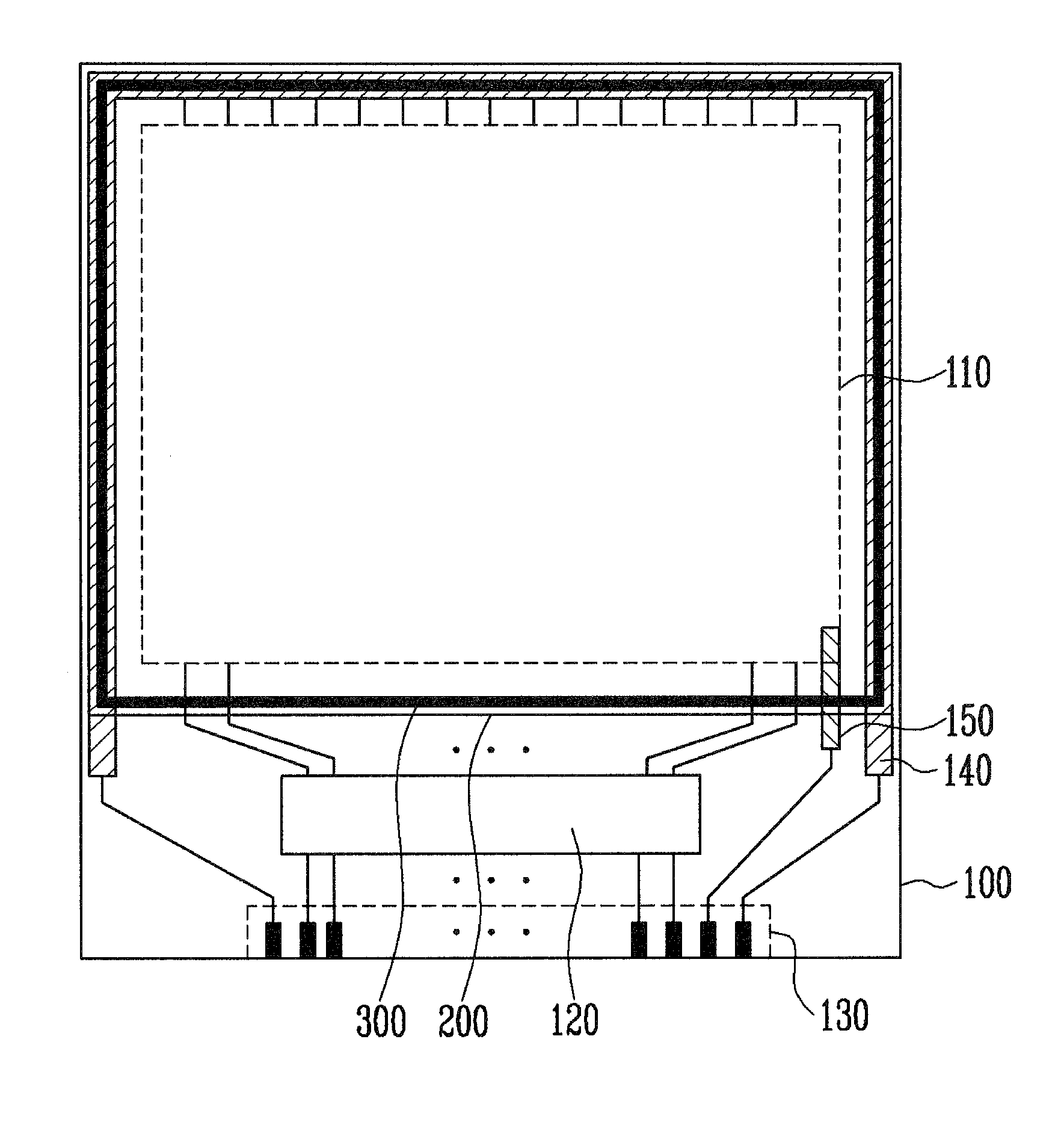
[0040]FIG. 1 is a plan view showing an organic light emitting display device according to an exemplary embodiment of the present invention.

[0041]Referring to FIG. 1, the organic light emitting display device according to an exemplary embodiment of the present invention includes a first substrate 100 having a display unit 110, a drive circuit 120 and a pad unit 130 formed thereon; a second substrate 200 disposed on one region of the first substrate 10...


PUM

PropertyMeasurementUnit
Forceaaaaaaaaaa
Poweraaaaaaaaaa
Electrical resistanceaaaaaaaaaa

Abstract

An organic light emitting display device. The organic light emitting display device includes a first substrate, a second substrate overlapping with at least one region of the first substrate and a sealing agent attached between the first substrate and the second substrate to seal a display unit therebetween. A conductive wire on the first substrate overlapping with at least a portion of the sealing agent includes a first conductive layer and a second conductive layer having at least one region formed at different levels to be electrically coupled to each other through contact holes. The first conductive layer and the second conductive layer are configured to reduce a resistance of the conductive wire and improve an adhesive force of the sealing agent.

Description

CROSS-REFERENCE TO RELATED APPLICATION[0001]This application claims priority to and the benefit of Korean Patent Application No. 10-2008-0018312, filed on Feb. 28, 2008, in the Korean Intellectual Property Office, the entire content of which is incorporated herein by reference.BACKGROUND OF THE INVENTION[0002]1. Field of the Invention[0003]The present invention relates to an organic light emitting display device, and more particularly, to a conductive wire and a sealing agent of an organic light emitting display device.[0004]2. Description of Related Art[0005]In recent years, there have been developed various flat panel displays that are light-weight and small-sized as compared with cathode ray tubes. Among the flat panel display devices, the organic light emitting display device has excellent luminance and color purity by using an organic compound as a light emitting material.[0006]An organic light emitting display device includes a display unit including a large number of pixels d...

Claims


Application Information

Patent Timeline
IPC IPC(8): H01J1/88
CPCH01L51/5246H01L27/3276Y02E10/549H10K59/131H10K50/8426H01L21/67126H05B33/26H10K77/10H10K10/84
Inventor KWAK, WON-KYU
Owner SAMSUNG DISPLAY CO LTD
Why Eureka
Try Eureka