Correlated double sampling circuit and sample hold circuit

Active Publication Date: 2009-09-03
PANASONIC SEMICON SOLUTIONS CO LTD
View PDF9 Cites 17 Cited by
  • Summary
  • Abstract
  • Description
  • Claims
  • Application Information

AI Technical Summary

Benefits of technology

[0019]As has been described above, a correlated double sampling circuit according to the invention is capable of reducing high

Problems solved by technology

In recent image sensors having improved resolution and higher read frequency, high quality image signal processing is di

Method used


Image

  • Correlated double sampling circuit and sample hold circuit
  • Correlated double sampling circuit and sample hold circuit
  • Correlated double sampling circuit and sample hold circuit

Examples


first embodiment

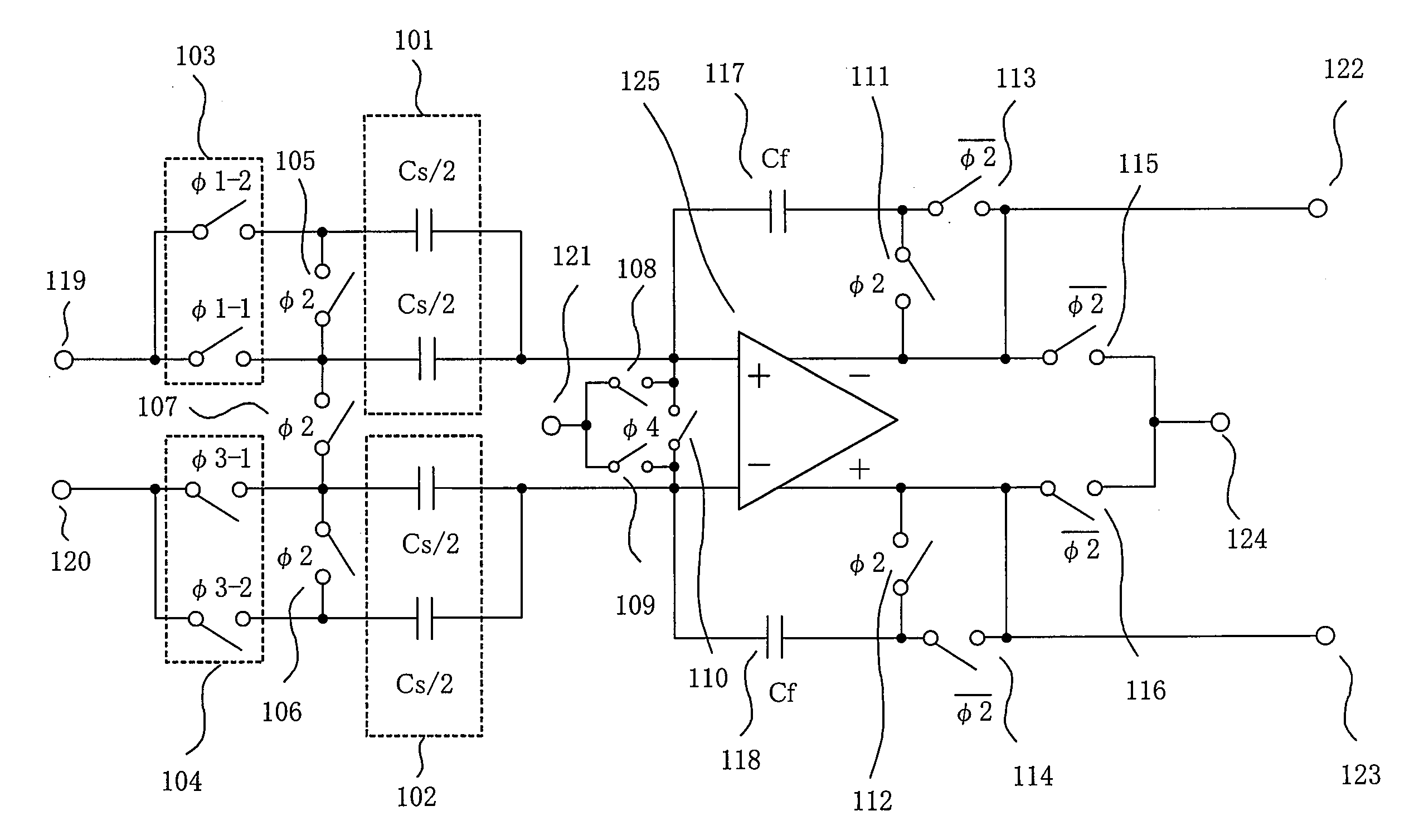
[0057]FIG. 1 shows a structure of a correlated double sampling circuit according to a first embodiment of the invention. It is herein assumed that each sampling capacitor in the correlated double sampling circuit is equally divided into two portions.

[0058]In FIGS. 1, 101 and 102 indicate sampling capacitors, 103, 104, and 107 through 116 indicate switch elements, 117 and 118 indicate feedback capacitors, 119 and 120 indicate input terminals, 122 and 123 indicate output terminals, 125 indicates an operational amplifier, 121 indicates an input terminal, and 124 indicates an output terminal.

[0059]As shown in FIG. 1, a signal of a feed-through portion of an image sensor output signal is applied to an input terminal 119 of the correlated double sampling circuit, and a signal of a data portion of the image sensor output signal is applied to an input terminal 120 of the correlated double sampling circuit.

[0060]Each sampling capacitor 101, 102 is equally divided into two portions, and a cap...

second embodiment

[0072]FIG. 4 shows a structure of a correlated double sampling circuit according to a second embodiment of the invention. The correlated double sampling circuit of FIG. 4 is obtained by applying characteristics of the invention to a conventional correlated double sampling circuit having a sample hold circuit 904 on the side of sampling a feed-through portion of an image sensor output signal as shown in FIG. 9. In other words, the correlated double sampling circuit of FIG. 4 is obtained by applying a method of equally dividing each sampling capacitor into N portions (where N is an integer of at least 2) to the conventional correlated double sampling circuit of FIG. 9.

[0073]As shown in FIG. 4, a sampling capacitor 403 of a sample hold circuit 407 is equally divided into N portions (where N is an integer of at least 2), and a capacitance value of each portion is Csh / N. In FIG. 4, 401 indicates a sampling switch, 404 indicates a switch element, 405 indicates an input terminal, and 406 i...


PUM


Abstract

A correlated double sampling circuit has a sampling capacitor equally divided into a plurality of portions. In the correlated double sampling circuit, an input signal is sampled at a plurality of sampling points and an averaging switch is closed to obtain an average value of a plurality of sampling values obtained by sampling. High frequency noise superimposed on the input signal is thus reduced and a difference between the average values of the plurality of sampling values obtained by sampling is output.

Description

TECHNICAL FIELD[0001]The invention relates to a correlated double sampling circuit and a sample hold circuit.BACKGROUND ART[0002]Conventionally, an analog image signal processing circuit such as a mobile phone camera and a digital still camera generally uses a single-ended structure and a differential structure in order to remove common mode noise such as disturbance. An output signal of an image sensor such as a CCD (Charge Coupled Device) and a CMOS (Complementary Metal-Oxide Semiconductor) sensor is sampled by a correlated double sampling circuit and then transmitted to an amplifier of a subsequent stage.[0003]In recent image sensors having improved resolution and higher read frequency, high quality image signal processing is difficult due to degraded S / N (Signal-to-Noise ratio) when high frequency noise is superimposed on a sensor output signal.[0004]FIG. 7 shows a structure of a conventional correlated double sampling circuit. FIG. 8 is a timing chart of the conventional correl...

Claims


Application Information

Patent Timeline
IPC IPC(8): G11C27/02H04N5/357H04N5/378
CPCH04N5/378H04N5/3575H04N25/616H04N25/75
Inventor OHBA, MAKOTO
Owner PANASONIC SEMICON SOLUTIONS CO LTD
Why Eureka
Try Eureka