InAs/GaSb Infrared Superlattice Photodiodes Doped with Beryllium

a superlattice and photodiode technology, applied in the field of photodiodes, can solve the problems of limited performance and small dark current at high temperatures of inas/gasb superlattice, and achieve the effect of improving the overall performance of the device and increasing the quantum efficiency of the devi

Active Publication Date: 2009-09-10
NORTHWESTERN UNIV
View PDF2 Cites 26 Cited by
  • Summary
  • Abstract
  • Description
  • Claims
  • Application Information

AI Technical Summary

Benefits of technology

[0006]Doping the π-region of the active layer of a long wavelength photodiode at 77 K with Beryllium (Be) has been shown to improve the overall performance of the device. First, by switching from a residually n-type to a p-type background, the quantum efficiency of the device is increased. Second, the R0A product can linearly increase with the doping level until the point where the diodes are dominated by band-to-band tunneling. Minimization of the dark current leads to an increase of the zero-bias differential resistance from less than 4 Ω·cm2 to 32 Ω·cm2 for a 100% cutoff of 12.05 μm.

Problems solved by technology

Furthermore, a reduced Auger recombination rate results in small dark current at high temperatures.
When operating at 77 K, the performance of an InAs / GaSb superlattice is limited by defect-assisted tunneling.

Method used


Image

  • InAs/GaSb Infrared Superlattice Photodiodes Doped with Beryllium
  • InAs/GaSb Infrared Superlattice Photodiodes Doped with Beryllium
  • InAs/GaSb Infrared Superlattice Photodiodes Doped with Beryllium

Examples


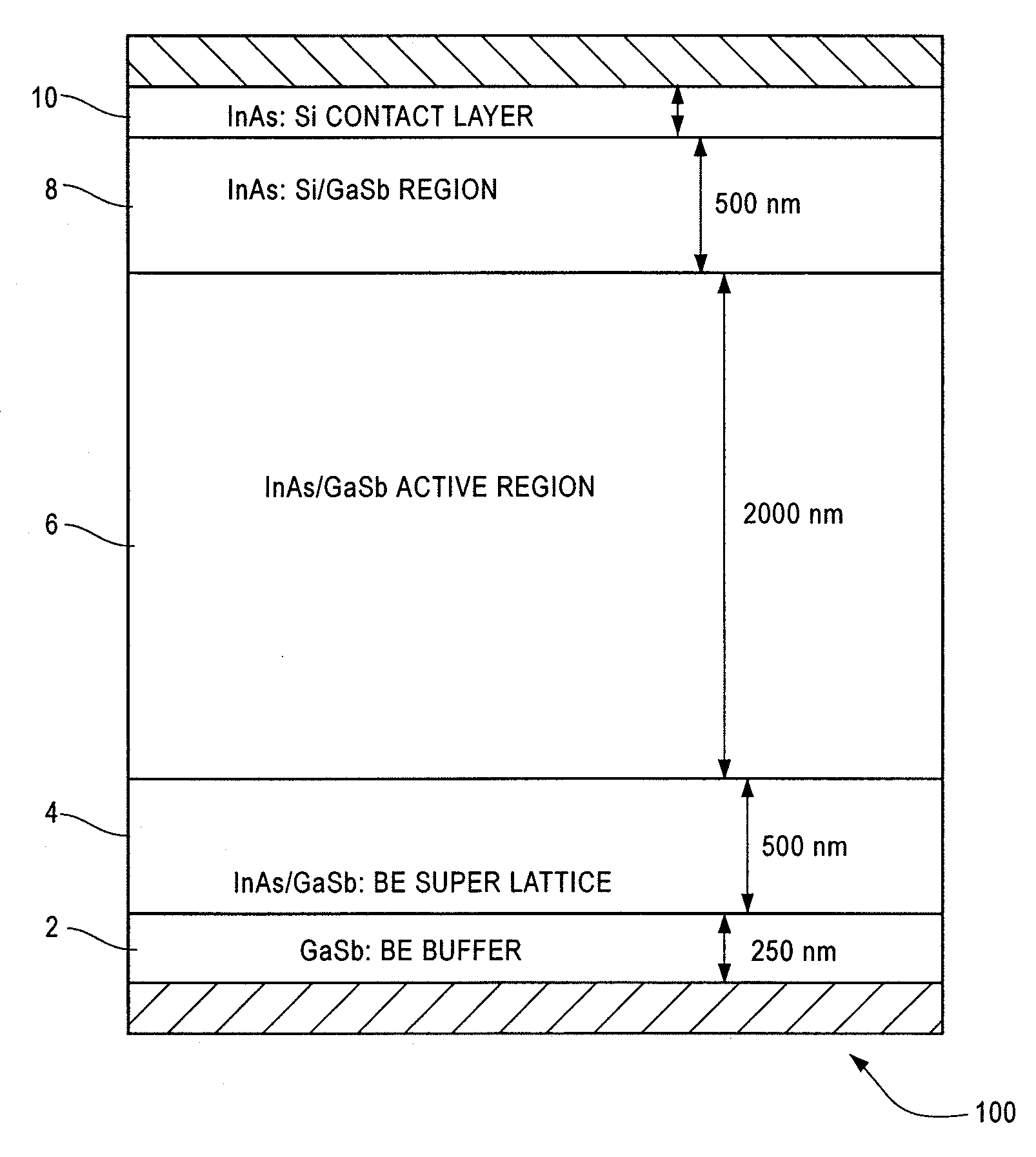
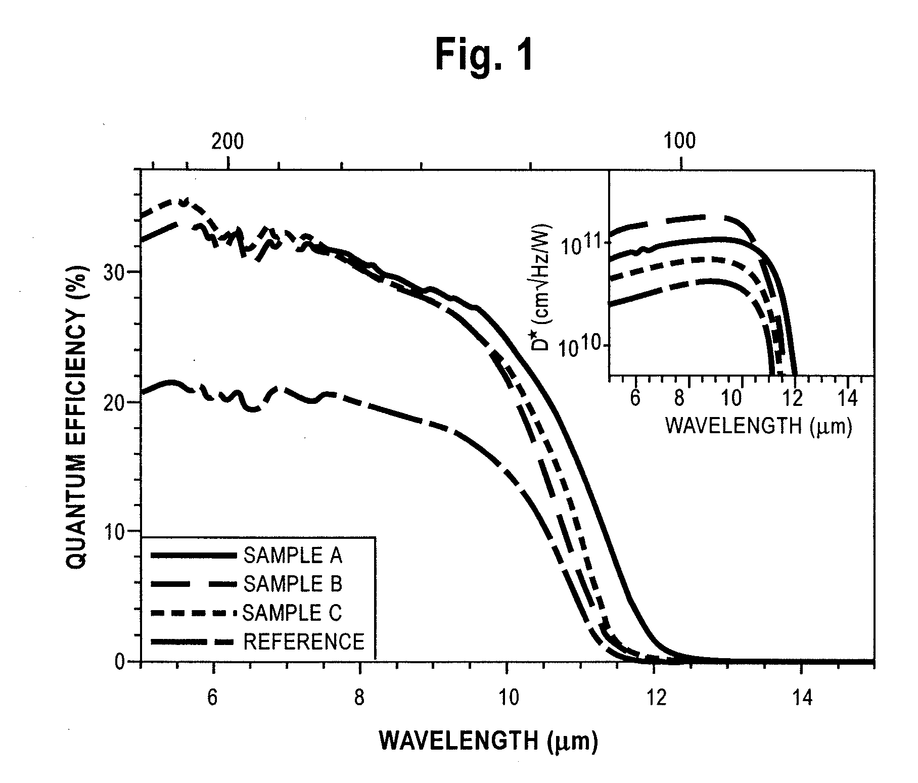
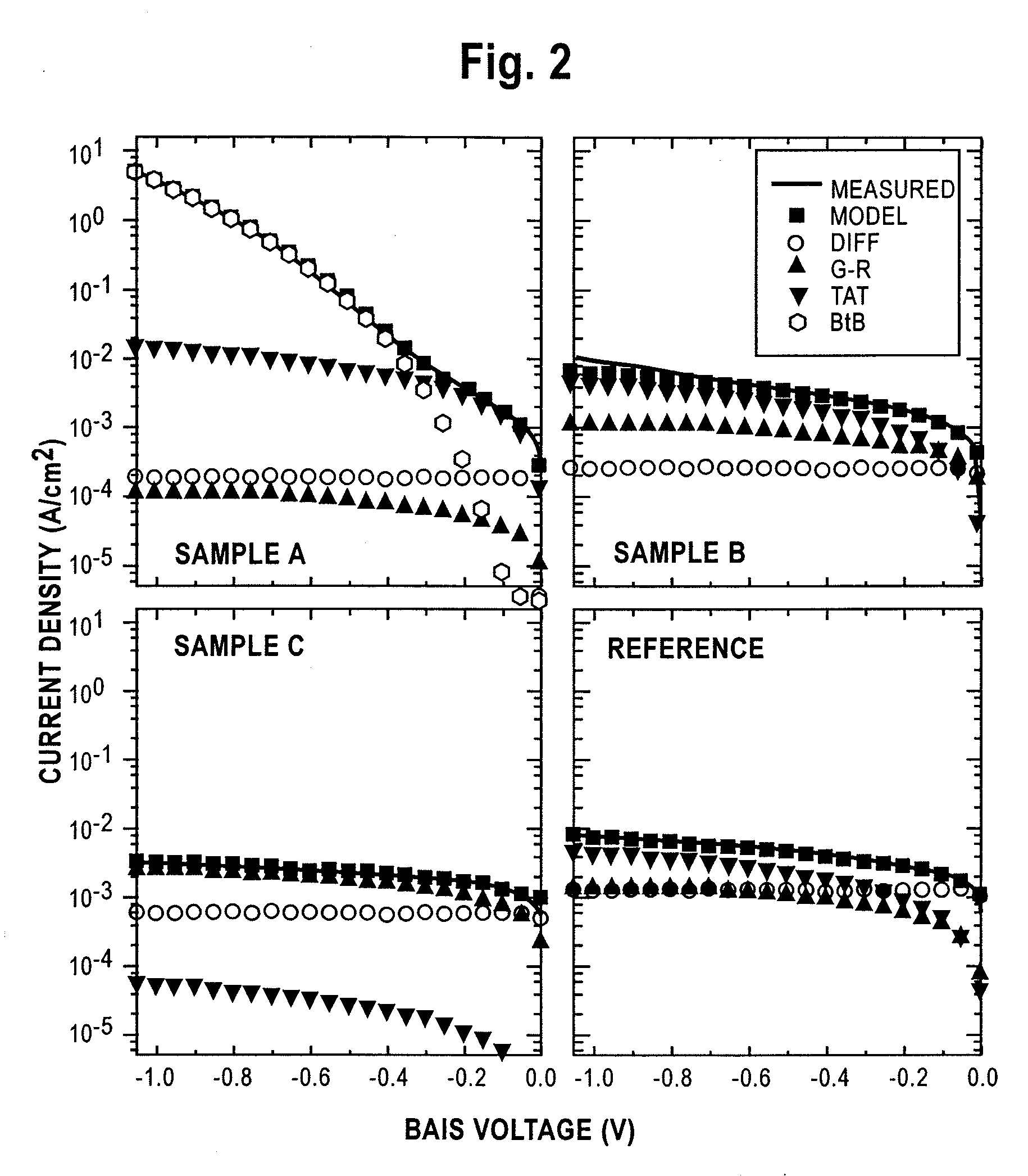
Embodiment Construction

[0012]While the present invention is susceptible of embodiments in various forms, there is shown in the drawings a number of presently preferred embodiments that are discussed in greater detail hereafter. It should be understood that the present disclosure is to be considered as an exemplification of the present invention, and is not intended to limit the invention to the specific embodiments illustrated. It should be further understood that the title of this section of the present application (“Detailed Description of the Invention”) relates to a requirement of the United States Patent Office, and should not be found to limit the subject matter disclosed herein.

[0013]Each of the articles cited herein is incorporated by reference. The use of the article “a” or “an” is intended to include one or more.

[0014]The foregoing description is intended as illustrative and is not to be taken as limiting. Still other variations within the spirit and scope of this invention are possible and will...


PUM


Abstract

An improved photodiode and method of producing an improved photodiode comprising doping an InAs layer of an InAs/GaSb region situated on top of an InAs/GaSb:Be superlattice and below an InAs:Si/GaSb regions such that the quantum efficiency of the photodiode increases and dominant dark current mechanisms change from diffusion to band-to-band tunneling as the InAs layer is doped with Beryllium.

Description

FIELD OF THE INVENTION[0001]The present invention relates generally to the field of photodiodes and more particularly to doping infrared superlattice photodiodes to improve the performance of the device.BACKGROUND OF THE INVENTION[0002]A superlattice (SL) is a structure consisting of closely spaced quantum wells, such that the localized discrete energy levels in the quantum wells become delocalized minibands across the entire structure, in both the conduction and valence bands. These minibands thus form an effective bandgap (Ege) for the superlattice considered as a whole.[0003]Type II superlattice systems are attractive to groups with both research and commercial interests because, for example, (1) the minibands of the superlattice can exhibit a lower effective bandgap than the bandgap of either constituting layer, (2) the electrons and holes are spatially separated, and (3) electrons can easily tunnel from the conduction band of one layer to the valence band of the other layer (i....

Claims


Application Information

Patent Timeline
Patent Type & Authority Applications(United States)
IPC IPC(8): H01L31/0352H01L29/15
CPCB82Y20/00H01L31/109H01L31/035236
Inventor RAZEGHI, MANIJEH
Owner NORTHWESTERN UNIV
Why Eureka
Try Eureka