

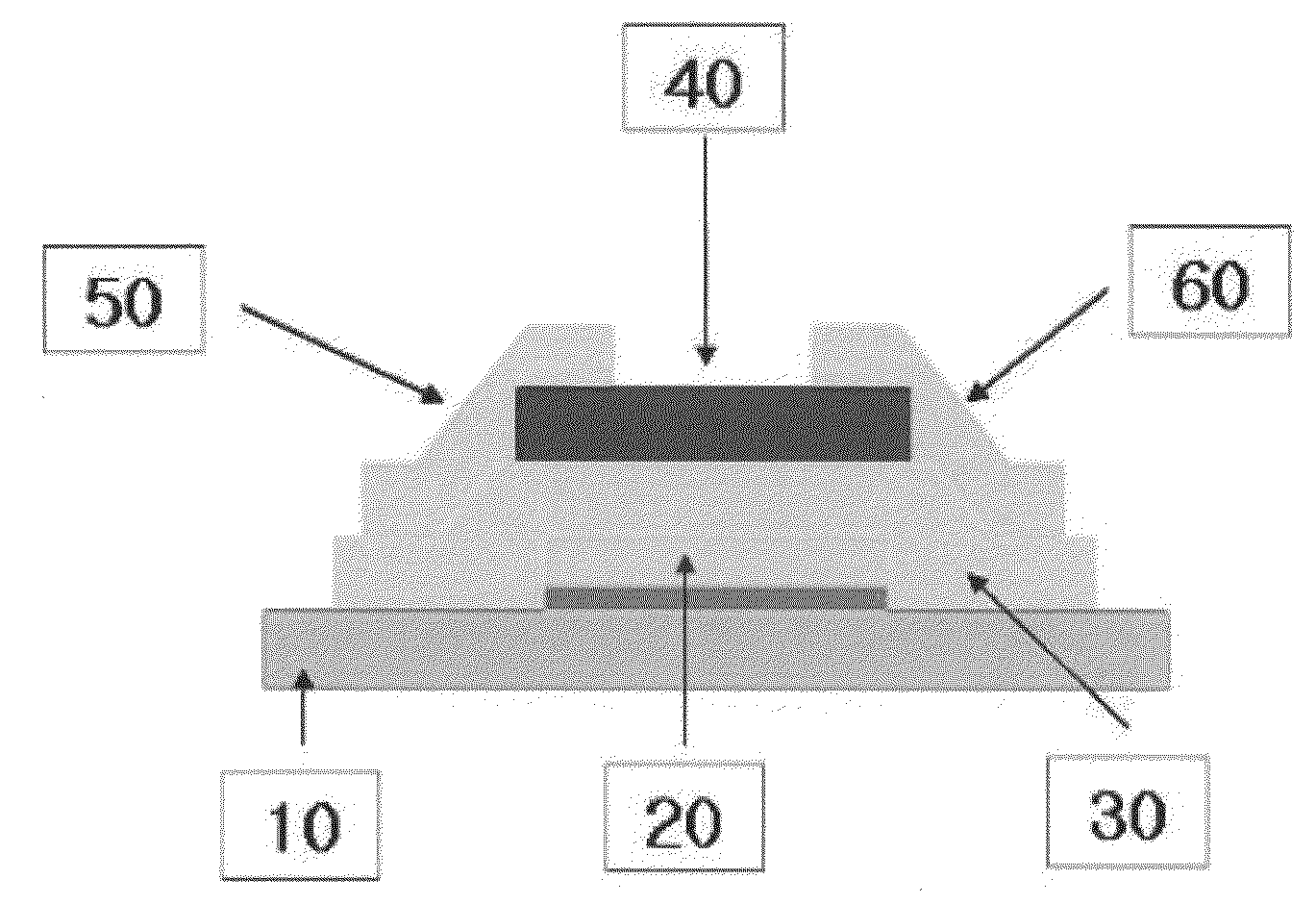
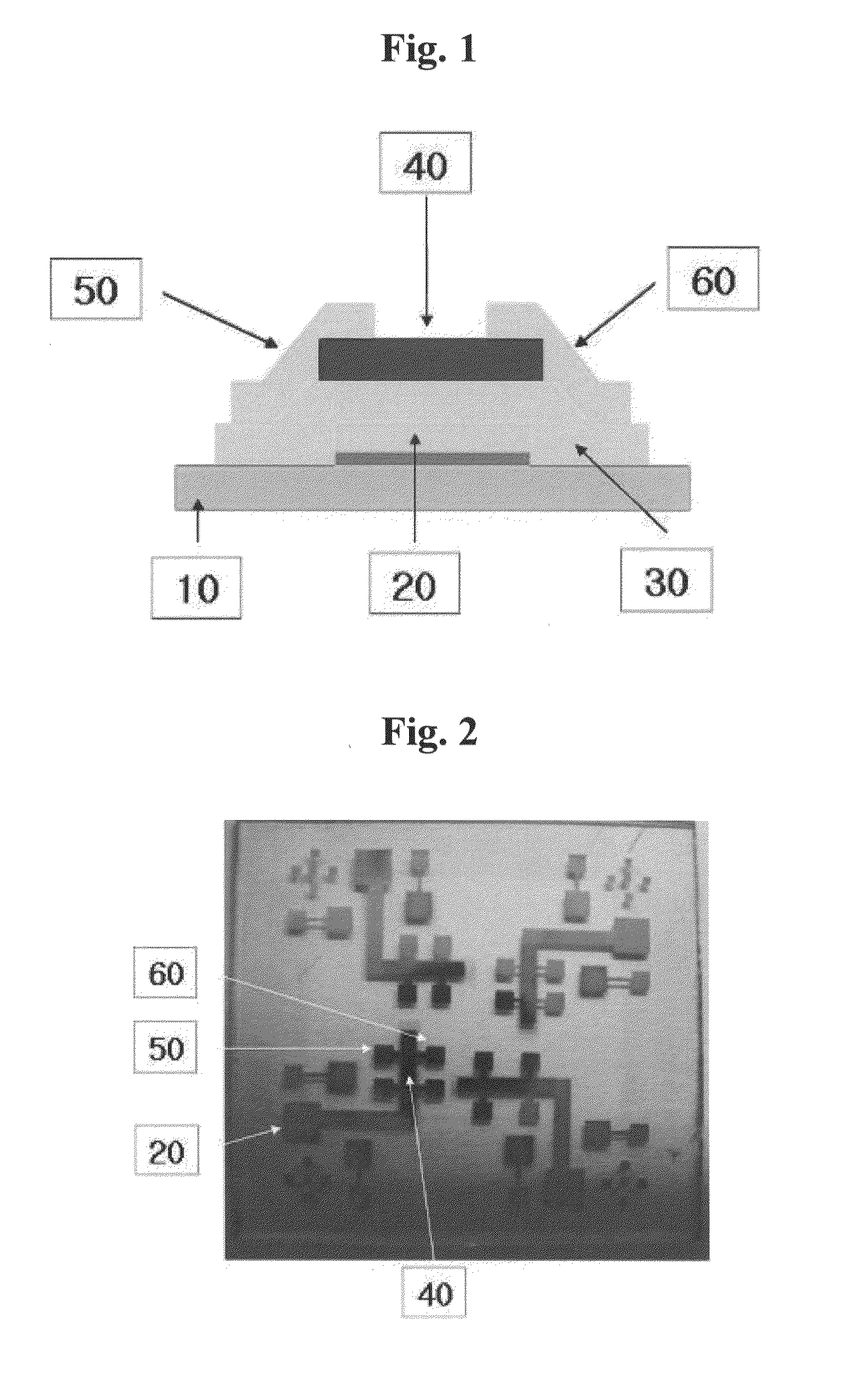
Organic thin film transistors including metal oxide nanoparticles within a photocurable transparent polymer gate insulator layer and method for fabricating the same by using sol-gel and photocuring reactions
a transparent polymer and gate insulator technology, applied in the field of organic thin film transistors, can solve the problems of difficult to fabricate a gate insulator layer with a high permittivity, low on/off current ratio, low charge carrier mobility, etc., and achieve low leakage current, easy to fabricate, and high on/off current ratio
- Summary
- Abstract
- Description
- Claims
- Application Information
AI Technical Summary
Benefits of technology
Problems solved by technology
Method used
Image

Examples
example 1
[0056]0.8 g of titanium n-butoxide (Aldrich) and 0.235 g of acetylacetone (Aldrich) were mixed at room temperature by stirring with a magnetic bar for 1 hour. 8.454 g of UV-cured acrylic resin (Dongjin Semichem Co., Ltd) was successively added thereto and mixed for 2 hours by stirring. To the resulting mixture was added 0.08247 g of 0.1 N HCl (Junsei), which was dispersed by stirring and ultrasonication for 1 hour, to obtain a coating solution. The coating solution was subjected to spin-casting for 30 seconds at a rate of 200 rpm on a glass substrate in which gold (Au) was deposited as a gate electrode in a thickness of 200 nm, to thereby form a transparent organic film. The glass substrate on which the above transparent organic film was formed was subjected to a sol-gel reaction by heating it in an oven at 100° C. for 20 minutes. After the sol-gel reaction was completed, the glass substrate was photocured by using a UV lamp (365 nm) at a dose of 300 mJ, followed by post-curing at 1...
example 2
[0061]An organic thin film transistor was fabricated by etching an ITO glass substrate and using it as a gate electrode according to the same conditions as described in Example 1.
example 3
[0062]An organic thin film transistor was fabricated according to the same conditions as described in Example 1, except that a PES substrate was used instead of a glass substrate.
PUM
| Property | Measurement | Unit |
|---|---|---|
| temperature | aaaaa | aaaaa |
| wavelength | aaaaa | aaaaa |
| particle size | aaaaa | aaaaa |
Abstract
Description
Claims
Application Information