Manufacturing method for field-effect tube and field-effect tube

A manufacturing method and technology of field effect transistors, applied in semiconductor/solid-state device manufacturing, semiconductor devices, electrical components, etc., can solve problems such as high cost and complicated process, achieve surface damage removal, increase mobility, and achieve ultra-steep sub- Effect of Threshold Swing

Inactive Publication Date: 2019-06-18
SHANGHAI IND U TECH RES INST
View PDF7 Cites 4 Cited by
  • Summary
  • Abstract
  • Description
  • Claims
  • Application Information

AI Technical Summary

Problems solved by technology

So far, the reported processes for fabricating SiGe nanowires are complicated, and the Damaccus pseudo-gate process using Si / SiGe alternating epitaxy is expensive, and the size reduction of nanowires has certain limitations.

Method used


Image

  • Manufacturing method for field-effect tube and field-effect tube
  • Manufacturing method for field-effect tube and field-effect tube
  • Manufacturing method for field-effect tube and field-effect tube

Examples


Embodiment Construction

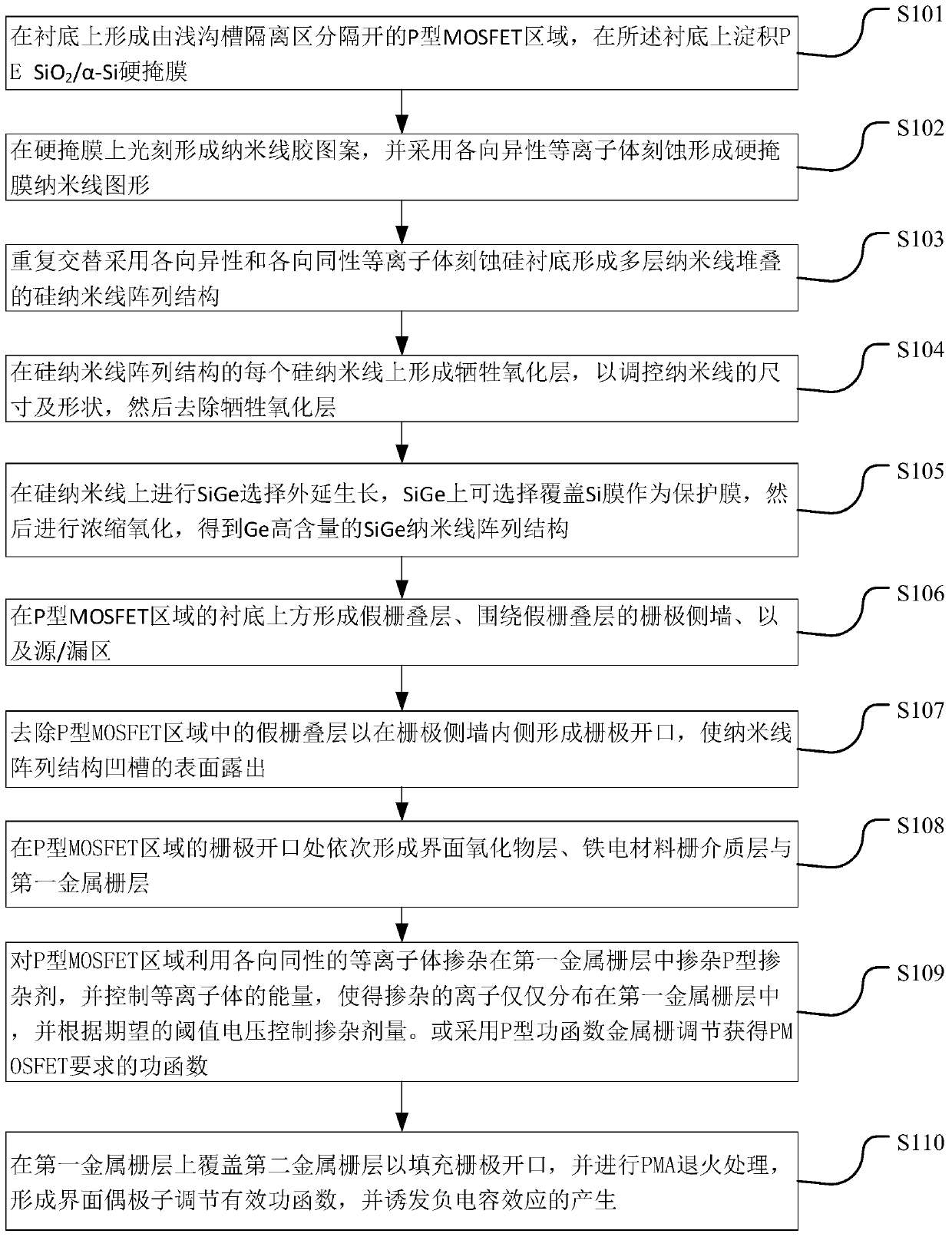
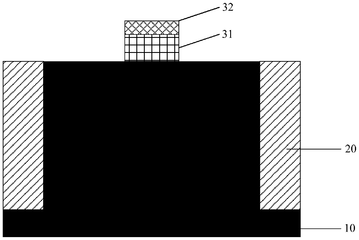
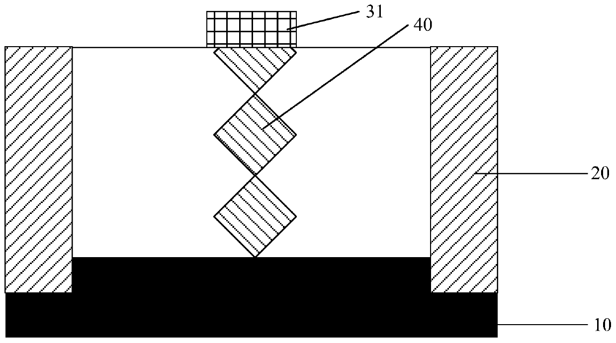
[0073] The present disclosure is to provide a manufacturing method of a field effect tube and a field effect tube. The SiGe nanowire ring gate PMOSFET improves the hole mobility, and at the same time, the compressive stress on the channel generated by the SiGe source / drain further improves the hole mobility. . Moreover, the gate-around structure of the nanowires greatly improves the gate control ability, and suppresses the short channel effect extremely well. In particular, the nanowire array gate-enclosed PMOSFET structure of the present disclosure integrates the negative capacitance effect, effectively increases the surface potential of the device channel, and makes it greater than the external gate voltage, that is, realizes the voltage amplification effect and breaks through the sub-threshold swing glass The Boltzmann limit realizes ultra-steep sub-threshold swing and higher on / off current ratio, meeting the requirements of high-performance PMOSFETs. Therefore, integratin...


PUM

PropertyMeasurementUnit
thicknessaaaaaaaaaa
thicknessaaaaaaaaaa
thicknessaaaaaaaaaa

Abstract

The invention discloses a manufacturing method for a field-effect tube and the field-effect tube. The method comprises the following steps of forming a P-type MOSFET region on a substrate, wherein theP-type MOSFET region is isolated by a shallow trench isolation area; forming a hard mask pattern in the P-type MOSFET region; forming a silicon nanowire array structure, wherein the silicon nanowirearray structure comprises multiple layers of stacked silicon nanowires; carrying out SiGe selective epitaxial growth and concentration oxidation on the silicon nanowires, and removing an oxidation layer to obtain an SiGe nanowire array structure; and sequentially forming an interface oxide layer, a ferroelectric material gate dielectric laminate and a metal gate laminate at the nanowire array structure. According to the field-effect tube, the gate control capability is greatly enhanced due to a fence structure, and the hole mobility is improved due to the PMOSFET SiGe nanowires, especially dueto the fact that a ferroelectric negative capacitance effect is introduced, the potential of the surface of a channel is amplified, so that a nanowire device has a super-steep sub-threshold slope andan improved on / off current ratio.

Description

technical field [0001] The disclosure belongs to the technical field of semiconductors, and relates to a manufacturing method of a field effect tube and the field effect tube. Background technique [0002] As the feature size of integrated circuits becomes smaller and smaller, planar CMOS devices have encountered serious challenges, and various new device structures have emerged. The gate structure of devices has evolved from traditional planar single gates to double gates, triple gates, and completely wrapped channel. The gate-all-around structure, the gate-control ability and the ability to control the short channel effect are continuously enhanced, and the MOSFET with the nanowire gate-all-around structure (GAA) with quasi-ballistic transmission characteristics is widely used due to its strong gate control ability and the ability to reduce the size. Attach great importance to it and become a strong competitor in the technology generation of 3nm and below. However, when t...

Claims


Application Information

Patent Timeline
Patent Type & Authority Applications(China)
IPC IPC(8): H01L29/78H01L29/51H01L29/49H01L21/336
Inventor 徐秋霞胡正明陈凯
Owner SHANGHAI IND U TECH RES INST
Why Eureka
Try Eureka