Analog baud rate clock and data recovery

a digital baud rate clock and data recovery technology, applied in the field of analog baud rate muellermuller algorithm based clock and data recovery, can solve the problems of costing a lot of area and power, affecting the performance of the link, and affecting the quality of the clock recovery

Active Publication Date: 2009-09-10
ORACLE INT CORP
View PDF5 Cites 28 Cited by
  • Summary
  • Abstract
  • Description
  • Claims
  • Application Information

AI Technical Summary

Benefits of technology

[0011]One or more embodiments of the present invention involve an analog baud rate clock and data recovery apparatus comprising: a first track and hold circuit that delays a received signal by one unit interval to create an odd signal, a second track and hold circuit that delays the received signal by one unit interval to create an even signal; a first comparator circuit; and a second comparator circuit, wherein the first track and hold circuit outputs the odd signal to the first comparator circuit and the second comparator circuit; wherein the second track and hold circuit outputs the even signal to the first comparator circuit and the second comparator circuit; wherein the first comparator adds the odd signal to the even signal and outputs a first potential timing error, wherein the second comparator subtracts the odd signal and the even signal and outputs a second potential timing error signal, wherein a desired timing error signal is derived from the first and second potential timing error signals, and wherein the desired timing error signal is used to determine whether signal sampling is early or late.
[0012]One or more embodiments of the present invention involve an analog baud rate clock and data recovery apparatus comprising: a first comparator circuit; a second comparator circuit; a third comparator circuit; a fourth comparator circuit; a pair of track and hold circuits along a main data path that delay the signal creating an odd signal and an even signal in relation to each other and send the odd signal and the even signal to the first, second, third, and fourth comparators; a first track and hold circuit; and a second track and hold circuit, wherein the first and second track and hold circuits receive a signal from the pair of track and hold circuits along the main data path, wherein the first track and hold delays the even signal by one unit interval, wherein the second track and hold delays the odd signal by one unit interval, wherein the first track and hold outputs the delayed even signal to the first and second comparator circuits, wherein the second track and hold outputs the delayed odd signal to the third and fourth comparator circuits, wherein the first comparator subtracts the odd signal to the delayed even signal, wherein the second comparator adds the odd signal and the delayed even signal, wherein the third comparator subtracts the delayed odd signal to the even signal, wherein the fourth comparator adds the delayed odd signal and the even signal, and wherein a timing error signal is derived from the outputs of the comparators and used to determine whether signal sampling is early or late.
[0013]One or more embodiments of the present invention involve a method of implementing an analog baud rate clock and data recovery apparatus comprising: receiving a signal for a main data path at a pair of track and hold circuits; delaying the signal by at least half a clock cycle in relation to each of the track and hold circuits in the pair creating an even and odd signal; receiving the even and odd signal from the first and second track and hold circuits at a first, second, third, and fourth comparator and the even signal at a first track and hold circuit and the odd signal at a second track and hold circuit; delaying the even and the odd signal at the first and second track and hold circuits respectively; receiving the delayed even and odd signals at the first, second, third, and fourth comparators; subtracting the odd signal to the delayed even signal at the first comparator; adding the odd signal and the delayed even signal at the second comparator; subtracting the delayed odd signal to the even signal at the third comparator; adding the delayed odd signal and the even signal at the fourth comparator; and deriving a timing error signal from the outputs of the comparators and using the timing error signal to tell the apparatus if signal sampling is early or late.
[0014]One or more embodiments of the present invention involve a method of implementing an analog baud rate clock and data recovery apparatus comprising; receiving a signal from the main data path at a first and second track and hold circuits; aligning odd signal and even signals by applying clock signals with one unit interval difference; receiving the odd signal from the first track and hold at the first and second comparators and receiving the even signal from the second track and hold at the first and second comparator; adding the odd signal to the even signal and at the first comparator adds and outputting a first potential timing error; subtracting the odd signal and the even signal from the second comparator and outputting a second potential timing error signal; and deriving a correct timing error signal and using the correct timing error signal to determine whether signal sampling is early or late.

Problems solved by technology

Today internal circuits can run at 10's of Gbps, but the performance of the link is limited by the characteristics of the channel, namely, the electrical path from one IC die to the other.
Working with a received signal can pose the issues of clock recovery and optimum phase selection.
This method is costly both in area and power because PLLs are known to consume a relatively large amount depending on the application.
As the data rate goes up to 10 Gbps and above, it is no longer practical to do oversampling at the required timing accuracy.
However, for those applications, which at most have 10-12 lanes per ASIC, power, area and latency of the receiver are not major considerations and such applications can afford a fairly sophisticated MM-based CDR with lots of computation.
The big disadvantage of such approach is that it required two very fast ADC front end (6.25 Gbps), which consume lots of power and area.
In addition, the accuracy of timing extraction is limited by ADC quantization.

Method used


Image

  • Analog baud rate clock and data recovery
  • Analog baud rate clock and data recovery
  • Analog baud rate clock and data recovery

Examples


Embodiment Construction

[0027]Embodiments of the present disclosure will be presented below with reference to the drawings.

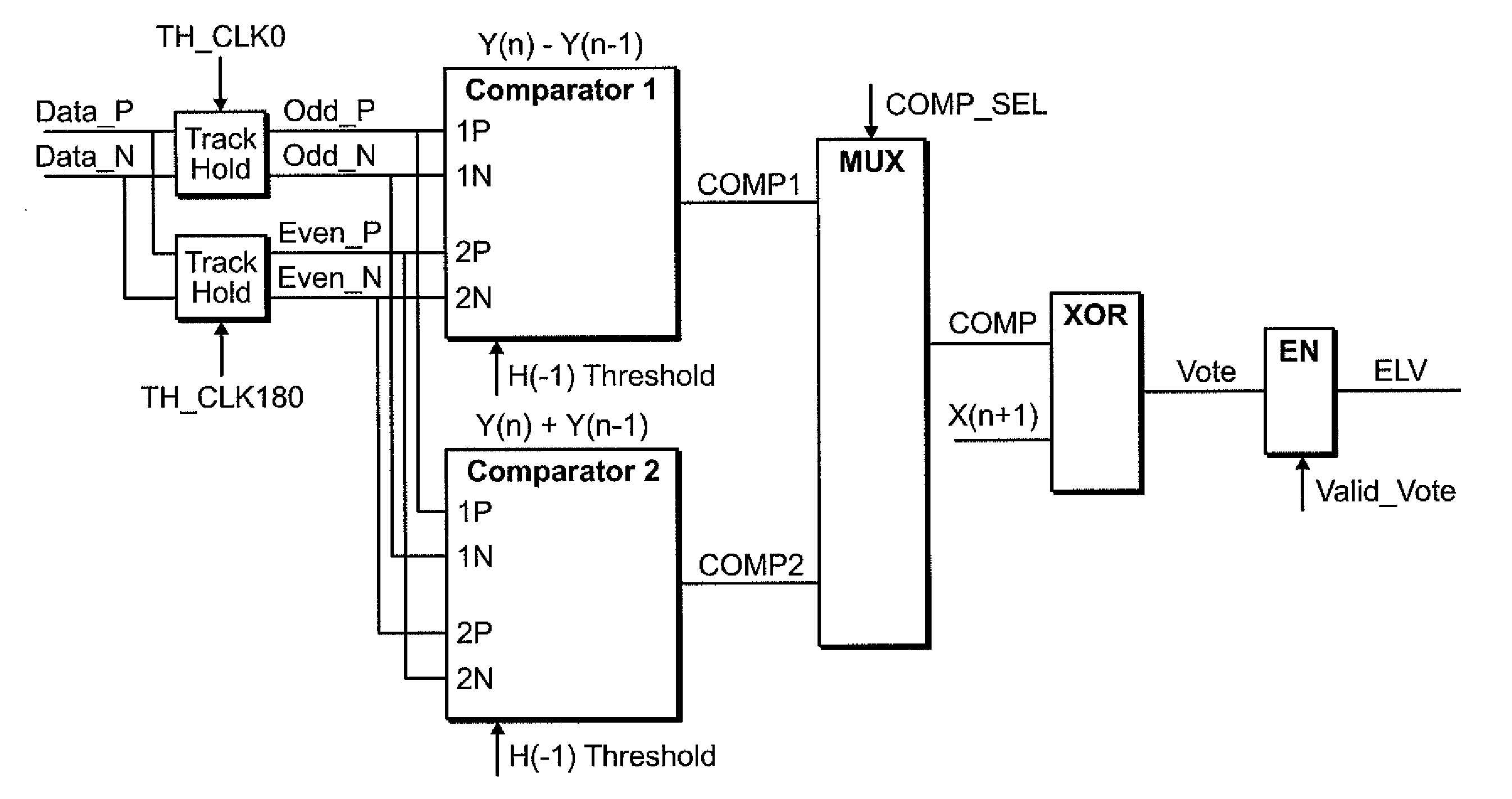
[0028]The Mueller-Muller (MM) algorithm set the theoretical framework for baud-rate CDR design However, the MM-algorithm does not cover the aspect of implementation with modern very-large-scale integration (VLSI) technology for specific applications. One or more embodiments of the present invention implement an analog baud-rate MM-based CDR.

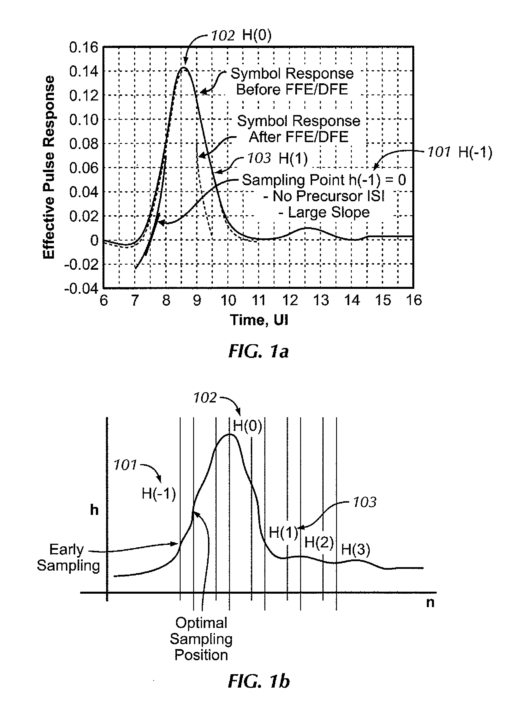
[0029]In one or more embodiments of the present invention, for a baud-rate clock and data recovery (CDR) algorithm based on the MM-algorithm approach, an optimal sampling time is that which the precursor H(−1) 101 (also called a timing error signal) of a symbol response is equal to a set threshold. For example, in FIG. 1a, the threshold is set to zero, but this is not necessarily the case for all possible adaptations. It may be desirable to set the threshold to a value slight above zero along the symbol curve. If H(−1) 101 is less than the threshold...


PUM


Abstract

An analog baud rate clock and data recovery apparatus includes a first track and hold circuit that delays a received signal by one unit interval to create an odd signal; a second track and hold circuit that delays the received signal by one unit interval to create an even signal; a first comparator circuit; and a second comparator circuit. The first track and hold circuit outputs the odd signal to the first comparator circuit and the second comparator circuit. The second track and hold circuit outputs the even signal to the first comparator circuit and the second comparator circuit. The first comparator adds the odd signal to the even signal and outputs a first potential timing error. The second comparator subtracts the odd signal and the even signal and outputs a second potential timing error signal. A desired timing error signal is derived from the first and second potential timing error signals. The desired timing error signal is used to determine whether signal sampling is early or late.

Description

BACKGROUND OF THE DISCLOSURE[0001]1. Field of the Disclosure[0002]Embodiments of the present disclosure relate to an analog baud-rate Mueller-Muller algorithm based clock and data recovery (CDR).[0003]2. Description of the Related Art[0004]Integrated circuits (IC) may need to communicate with other ICs or modules in any given system design. The ever increasing processing and computation speed of ICs has created a growing demand for high-bandwidth input and output (IO) on these ICs, which is achieved by increasing the signaling rate of each IO pin as well as increasing the number of IO pins on the chip. Today internal circuits can run at 10's of Gbps, but the performance of the link is limited by the characteristics of the channel, namely, the electrical path from one IC die to the other. In order to achieve desired data rates over existing channels, many multi-Gbps links use complex signal processing to overcome the channel limitations. One such example for improving performance of ...

Claims


Application Information

Patent Timeline
Patent Type & Authority Applications(United States)
IPC IPC(8): H03K5/153
CPCH04L7/0062
Inventor HUANG, DAWEIQIN, ZUXUDOBLAR, DREW G.AHMAD, WASEEMYOON, DONG JOONJAVED, OSMAN
Owner ORACLE INT CORP
Why Eureka
Try Eureka