Method for Manufacturing Non-Volatile Memory Device having Charge Trap Layer

a non-volatile memory and charge trap technology, applied in the field of semiconductor devices, can solve the problems of reduced total effective dielectric constant, low dielectric constant of desired interfacial layer, and excessive generation of silicate or silicide layer

Inactive Publication Date: 2009-09-10
SK HYNIX INC
View PDF3 Cites 37 Cited by
  • Summary
  • Abstract
  • Description
  • Claims
  • Application Information

AI Technical Summary

Benefits of technology

[0006]In one embodiment of the invention, a method for manufacturing a non-volatile memory device having a charge trap layer comprises: forming a first dielectric layer over a semiconductor substrate; forming a second dielectric layer having a higher dielectric constant than that of the first dielectric layer over the first dielectric layer; forming a nitride buffer layer for preventing an interfacial reaction over the second dielectric layer; forming a third dielectric layer by supplying a radical oxidation source onto the nitride buffer layer to oxidize the nitride buffer layer, thereby forming a tunneling layer comprising the first, second, and third dielectric layers; and forming a charge trap layer, a shielding layer, and a control gate electrode layer over the tunneling layer.

Problems solved by technology

However, an undesired interfacial layer having low dielectric constant, e.g. a silicate layer or a silicide layer may be excessively generated in interface between the layers in the multilayer structure.
This interfacial layer of low dielectric constant may lead to reduction in total effective dielectric constant of the tunneling layer, and generation of the interfacial layer may cause undesirable, excessively increased roughness of the layers.
Therefore, the properties of entire tunneling layer as well as operation properties of the memory cell may deteriorate.

Method used


Image

  • Method for Manufacturing Non-Volatile Memory Device having Charge Trap Layer
  • Method for Manufacturing Non-Volatile Memory Device having Charge Trap Layer
  • Method for Manufacturing Non-Volatile Memory Device having Charge Trap Layer

Examples


Embodiment Construction

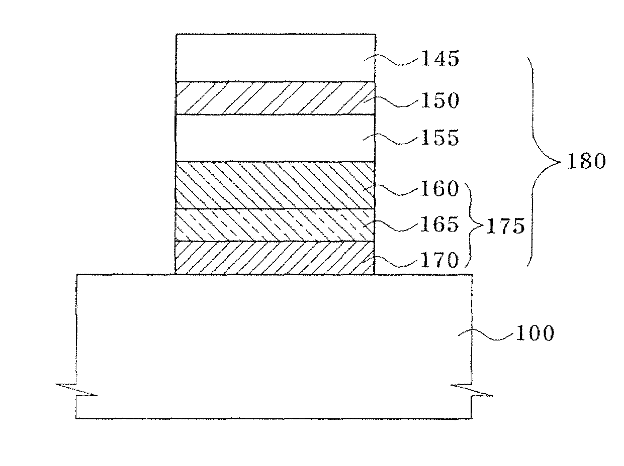
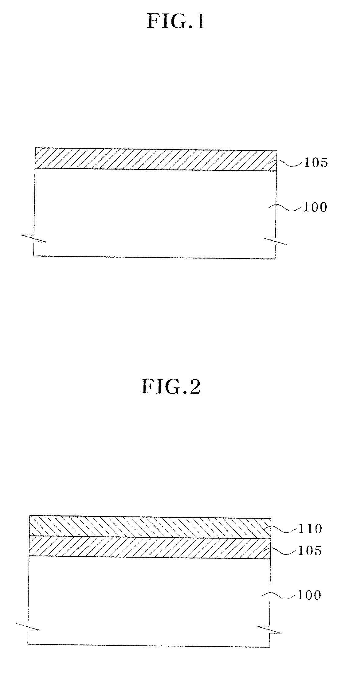
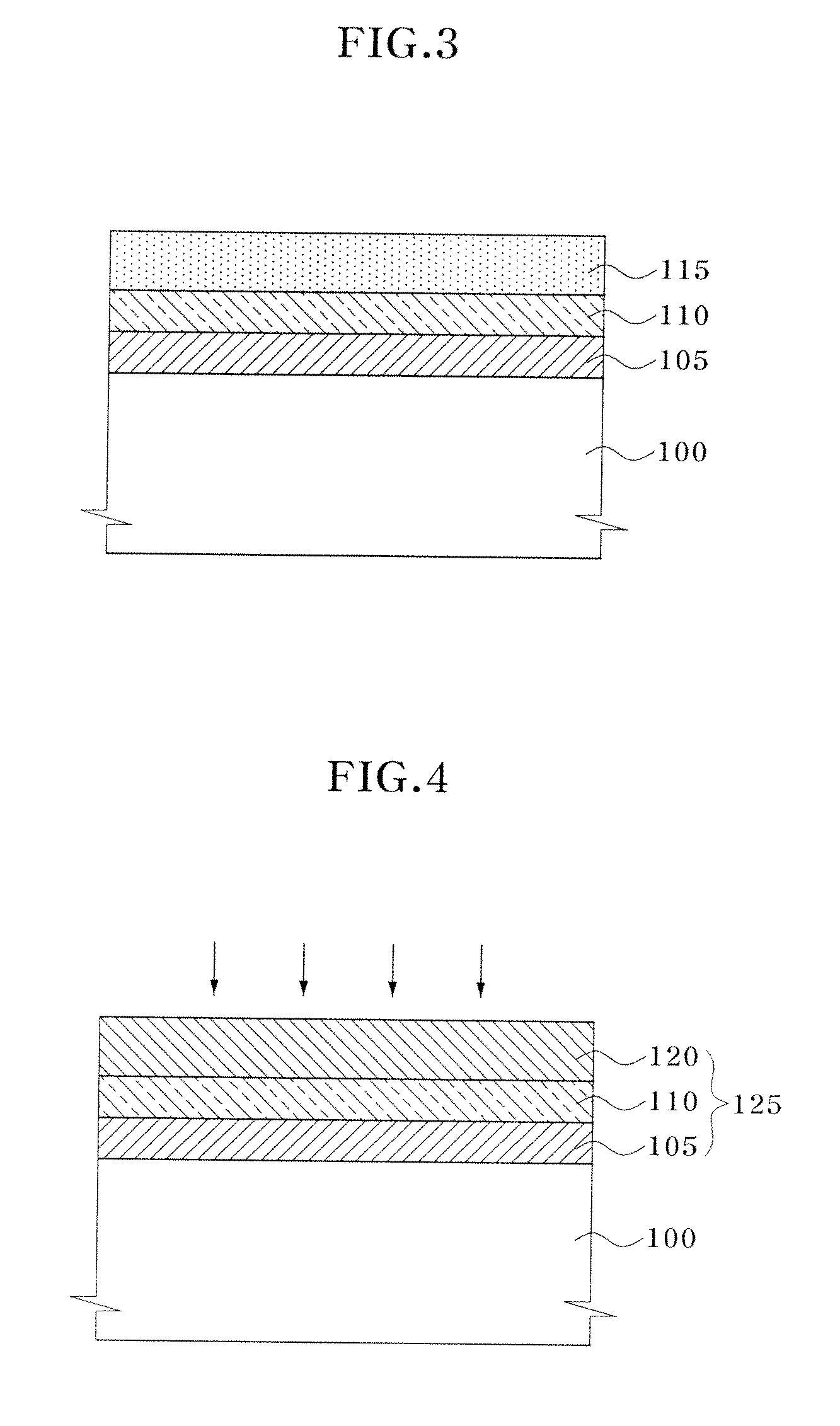
[0018]In a method for manufacturing a non-volatile memory device having a charge trap layer in accordance with an embodiment of the invention, a tunneling layer is formed in a multilayer structure including a dielectric material layer of a high dielectric constant, i.e. a high-k material layer. At this time, in order to inhibit excessive generation of an undesired interfacial layer having a relatively low dielectric constant in an interface between the high-k material layer and another, overlying dielectric material layer, a process of depositing a silicon nitride layer in a thin thickness (less than tens of Å) over the high-k material layer is utilized. The silicon nitride layer inhibits diffusion of oxygen from hafnium oxide (HfO2) or zirconium oxide (ZrO) or similar materials which are typically used as the high-k material layer and thus inhibits generation of the interfacial layer of silicate or silicide having a relatively low dielectric constant. After that, the silicon nitrid...


PUM


Abstract

A method for manufacturing a non-volatile memory device having a charge trap layer comprises in one embodiment: forming a first dielectric layer over a semiconductor substrate; forming a second dielectric layer having a higher dielectric constant than that of the first dielectric layer over the first dielectric layer; forming a nitride buffer layer for preventing an interfacial reaction over the second dielectric layer; forming a third dielectric layer by supplying a radical oxidation source onto the nitride buffer layer to oxidize the nitride buffer layer, thereby forming a tunneling layer comprising the first, second, and third dielectric layers; and forming a charge trap layer, a shielding layer, and a control gate electrode layer over the tunneling layer.

Description

CROSS-REFERENCE TO RELATED APPLICATION[0001]Priority to Korean patent application number 10-2008-0020700 filed on Mar. 5, 2008, the entire disclosure of which is incorporated by reference, is claimed.BACKGROUND OF THE INVENTION[0002]The invention relates generally to a semiconductor device and, more particularly, to a method for manufacturing a non-volatile memory device having a charge trap layer.[0003]Non-volatile memory devices are electrically programmable and erasable memory devices and are widely used in electronic components which require information to be maintained even when the power is not supplied. The non-volatile memory devices may be formed having a floating gate structure and information may be programmed or erased by injecting or removing a charge in the floating gate. As the degree of integration of memory devices increases, there has been suggested a non-volatile memory device structure in which a charge is injected or removed in a charge trap layer.[0004]In a non...

Claims


Application Information

Patent Timeline
Patent Type & Authority Applications(United States)
IPC IPC(8): H01L21/336
CPCH01L21/28282H01L29/792H01L29/513H01L29/40117H01L21/28202H01L29/4234H01L29/66833
Inventor JOO, MOON SIGCHO, HEUNG JAEKIM, YONG SOOCHOI, WON JOONWHANG, SUNG JIN
Owner SK HYNIX INC
Why Eureka
Try Eureka