Method for Producing Bonded Wafer, Bonded Wafer, and Surface Grinding Machine

a technology of surface grinding machine and bonded wafer, which is applied in the direction of manufacturing tools, semiconductor/solid-state device testing/measurement, transportation and packaging, etc., can solve the problems of complex process and inability to meet the quality requirements of recent years, and achieve high yield ratio, low cost, and reduce unevenness

Inactive Publication Date: 2009-09-17
SHIN-ETSU HANDOTAI CO LTD
View PDF1 Cites 2 Cited by
  • Summary
  • Abstract
  • Description
  • Claims
  • Application Information

AI Technical Summary

Benefits of technology

[0007]An object of the present invention is to provide a method for producing a bonded wafer which can reduce unevenness in thickness of a silicon single crystal thin film and precisely obtain a desired film thickness, and a bonded wafer; and a surface grinding machine which can precisely obtain a desired thickness of the silicon single crystal thin film as described above.
[0008]To achieve this object, according to the present invention, there is provided a method for producing a bonded wafer, comprising at least: bonding a base wafer serving as a support substrate to a bond wafer made of a silicon single crystal via an insulator film or directly bonding the wafers to provide a bonded wafer; and reducing a thickness of the bond wafer to form a thin film made of the silicon single crystal on the base wafer, wherein the thickness of the bond wafer is reduced based on at least surface grinding while measuring the thickness of the bond wafer, and surface grinding with respect to the bond wafer is stopped when the thickness of the bond wafer reaches a target thickness.
[0009]As described above, when the thickness of the bond wafer is reduced based on at least surface grinding while directly measuring the thickness of the bond wafer and surface grinding of the bond wafer is stopped at the moment the thickness of the bond wafer reaches a target thickness, the target thickness of the silicon single crystal thin film can be further precisely obtained without being affected by a measurement error in the thickness of the base wafer.

Problems solved by technology

However, when this method is adopted, unevenness in thickness of the obtained silicon single crystal thin film is large, the process is complicated, and quality requirements in recent years cannot be met.

Method used


Image

  • Method for Producing Bonded Wafer, Bonded Wafer, and Surface Grinding Machine
  • Method for Producing Bonded Wafer, Bonded Wafer, and Surface Grinding Machine
  • Method for Producing Bonded Wafer, Bonded Wafer, and Surface Grinding Machine

Examples


example 1

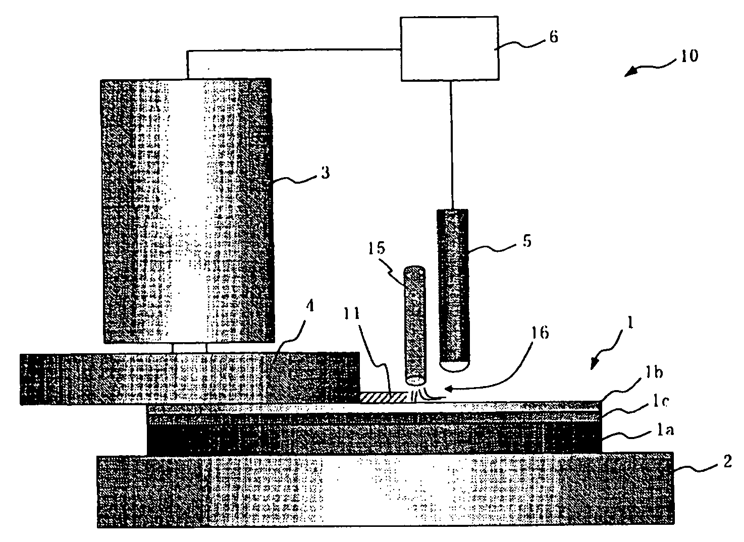
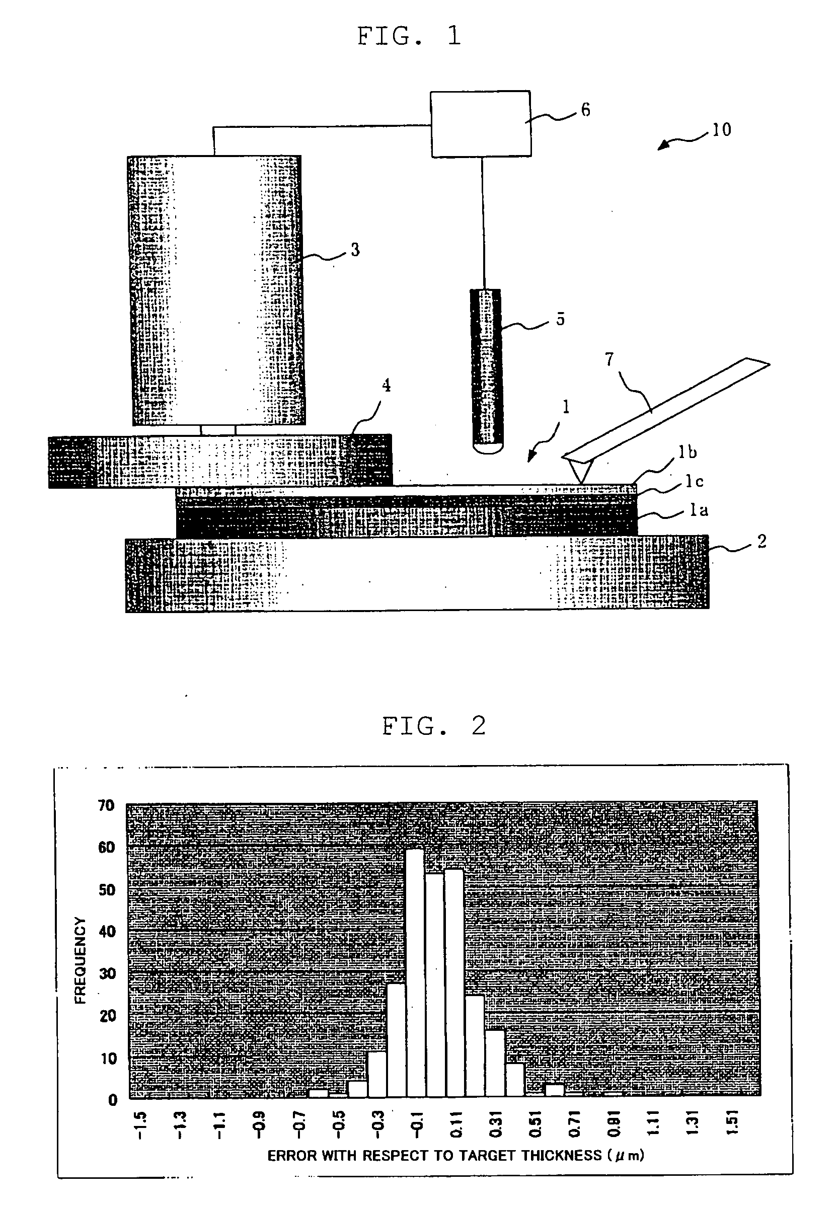
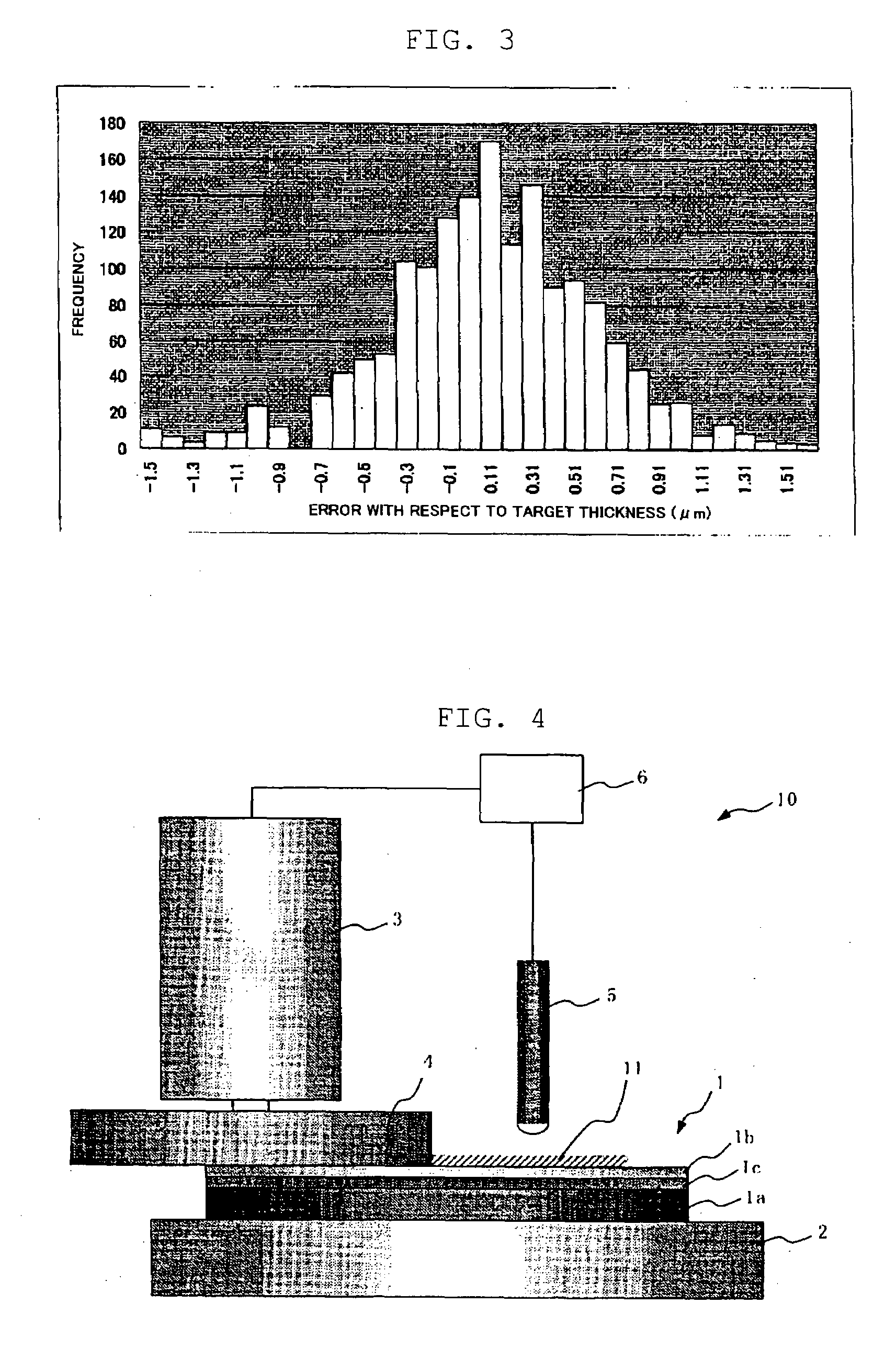
[0071]Two hundred sixty-five bonded wafers were fabricated, each bonded wafer having a structure where a base wafer which has a diameter of 200 mm and is made of a silicon single crystal is bonded to a bond wafer made of a silicon single crystal having a silicon oxide film formed on a surface thereof. Then, a machine obtained by combining a grinding machine DFG-840 manufactured by Disco Corporation, a general-purpose spectral reflectance measurement type film thickness meter, and a predetermined control mechanism was used as a surface grinding machine, Vitrified #325 was used as a coarse grinding wheel, Resin #2000 was used as a finishing grinding wheel, and the bond wafer of the bonded wafer was subjected to surface grinding to reduce its thickness. Surface grinding was carried out while measuring a thickness of the bond wafer (a thin film) by using the spectral reflectance measurement type film thickness meter. Further, at the same time, a general-purpose contact-type measurement ...


PUM

PropertyMeasurementUnit
thicknessaaaaaaaaaa
temperatureaaaaaaaaaa
thicknessaaaaaaaaaa

Abstract

The present invention is a method for producing a bonded wafer, comprising at least: bonding a base wafer serving as a support substrate to a bond wafer made of a silicon single crystal via an insulator film or directly bonding the wafers to provide a bonded wafer; and reducing a thickness of the bond wafer to form a thin film made of the silicon single crystal on the base wafer, wherein the thickness of the bonded wafer is reduced based on at least surface grinding while measuring the thickness of the bond wafer, and surface grinding with respect to the bond wafer is stopped when the thickness of the bond wafer reaches a target thickness. As a result, the method for producing a bonded wafer enabling a silicon single crystal thin film to precisely have a desired film thickness, a bonded wafer, and a surface grinding machine enabling a silicon single crystal thin film to precisely have a desired film thickness are provided.

Description

TECHNICAL FIELD[0001]The present invention relates to a method for producing a bonded wafer, a bonded wafer produced based on this method, and a surface grinding machine for use in formation of a thin film.BACKGROUND ART[0002]As a method of fabricating an SOI wafer having an SOI (Silicon On Insulator) structure in which a silicon layer is formed on an insulator, a method of fabricating a bonded SOI wafer by bonding two of silicon single crystal wafers, which are a base wafer serving as a support substrate and a bond wafer an SOI layer is to be formed, via a silicon oxide film is known. As a process of fabricating such a bonded wafer, for example, a method of forming an oxide film on a surface of at least one of two wafers, bringing the wafers into close contact with each other without interposing foreign matters on surfaces to be bonded and then performing a heat treatment at a temperature of approximately 200 to 1200° C. to enhance the bonding strength is known (see Japanese Examin...

Claims


Application Information

Patent Timeline
Patent Type & Authority Applications(United States)
IPC IPC(8): B24B49/04H01L21/66B24B49/12B32B9/00
CPCB24B7/228B24B49/12H01L22/26H01L21/76256H01L21/3212Y10T428/31663H01L21/20H01L21/304
Inventor OKABE, KEIICHITACHIKAWA, YOSHIKAZUMIYAZAKI, SUSUMUYOSHIZAWA, SIGEYUKITAKEI, TOKIO
Owner SHIN-ETSU HANDOTAI CO LTD
Why Eureka
Try Eureka