Gridded glyph geometric objects (L3GO) design method

a geometric object and glyph technology, applied in the field of circuit design, can solve the problems of large voltage drop or voltage spike, unreliable response of all features, unwanted short circuits or wiring neighboring circuits, etc., to improve layout data preparation efficiency, reduce cost and risk of layout generation, the effect of improving layout efficiency

Inactive Publication Date: 2009-09-17
GLOBALFOUNDRIES INC
View PDF9 Cites 50 Cited by
  • Summary
  • Abstract
  • Description
  • Claims
  • Application Information

AI Technical Summary

Benefits of technology

[0014]It is yet another purpose of the invention to reduce the cost and risk of layout generation and layout checking of circuits with arrays of inter-level contacts at selected inter-level connections;
[0015]It is yet another purpose of the invention to improve the efficiency of layout data preparation in designs with arrays of inter-level contacts at selected inter-level connections;
[0016]It is yet another purpose of the invention to improve the efficiency of layouts including and in using arrays of inter-level contacts in gridded glyph geometric objects (L3GO) format designs.
[0017]The present invention relates to a method of gridded glyph geometric objects (L3GO) integrated circuit (IC) design, wherein at least one inter-level connect in a L3GO circuit design is represented as a point matrix glyph (PMG) on a L3GO grid. Each PMG connects a pair of conductors on the next adjacent (above and below) layer and includes an array (one or two dimensional) of point glyphs contained within a cage. The point glyphs may have uniform size and may be on minimum pitch. Each PMG may also include a flange on the above and below layer. A default flange insures adequate coverage of cut shapes represented by the point glyphs.

Problems solved by technology

However, all features do not respond uniformly.
However, where relatively large currents flow through such a contact / via, this same contact resistance can cause relatively large voltage drops or voltage spikes (e.g., 20% of the supply voltage or more) that are very troublesome.
Unfortunately, different sized contact shapes and vias behave differently to focus and subsequent fabrication processing.
Consequently, this encroachment may cause unwanted shorts to those neighboring circuits or wiring.
Either result is undesirable, causing chips to fail and reducing chip yield.
Either of these results is undesirable and may cause failing chips, i.e., yield loss.
Unfortunately, using a point glyph alone (e.g., a point on a via layer) to represent vias, especially using multiple, redundant vias form a single connection, has been ineffective in capturing design intent.
Adding an array of point glyphs that may not allow a minimum pitch array has not proven effective either

Method used


Image

  • Gridded glyph geometric objects (L3GO) design method
  • Gridded glyph geometric objects (L3GO) design method
  • Gridded glyph geometric objects (L3GO) design method

Examples


Embodiment Construction

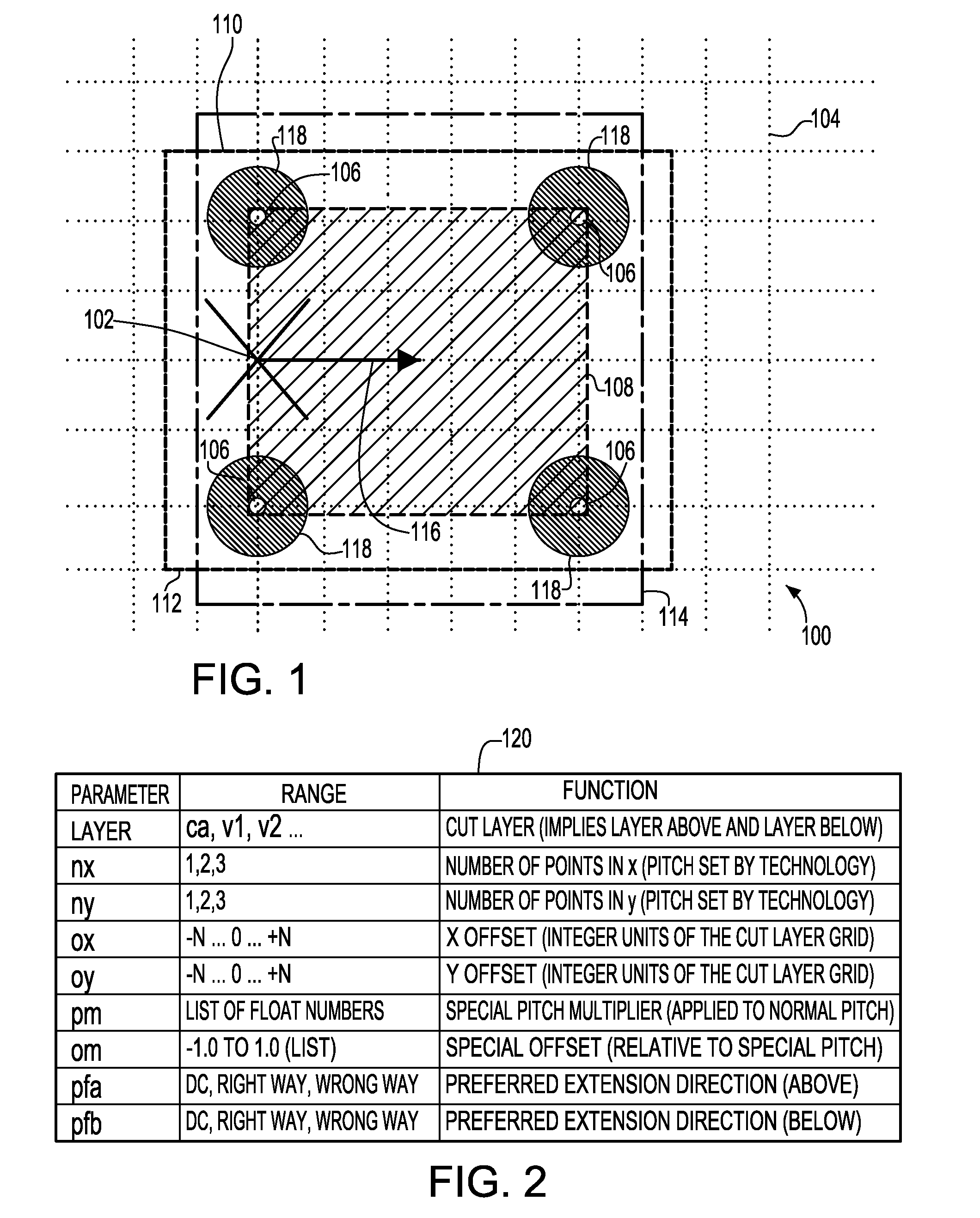
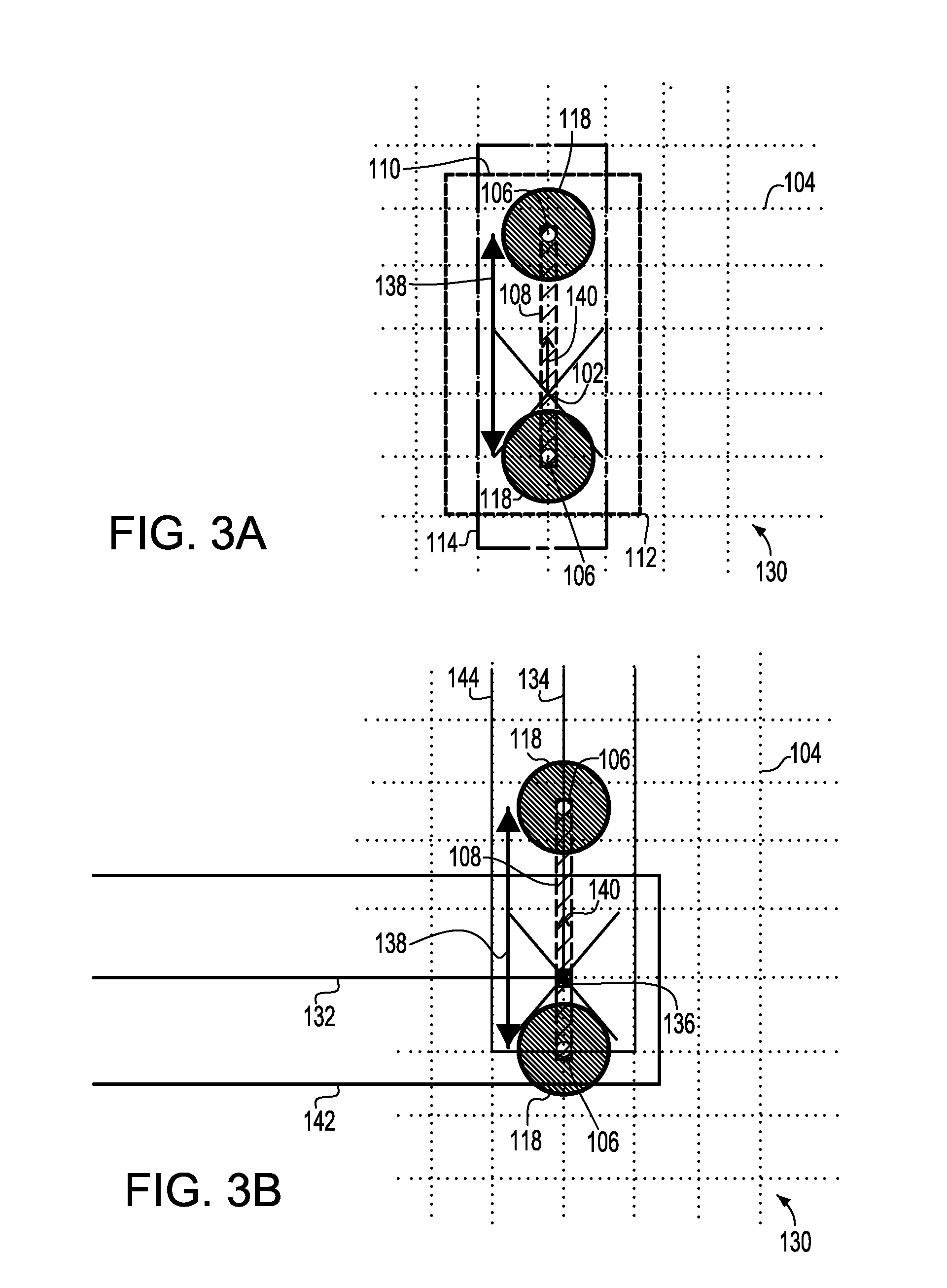
[0023]Turning now to the drawings and, more particularly, FIG. 1 shows a simple example of a point matrix glyph (PMG) 100 located at origin 102 on a grid point on a placement grid 104 in a gridded glyph geometric objects (L3GO) design, according to a preferred embodiment of the present invention. Preferably, a PMG 100 is a multi-layer cell-glyph that may be used to locate a via array connecting metal layers or a contact array, e.g., connecting metal to diffusion. In particular, PMGs 100 have application in circuit design, e.g., integrated circuit (IC) chip grid and glyph design, such as is described in Published U.S. patent application No. US 2006 / 0036977 A1, entitled “Physical Design System And Method” to Cohn et al., assigned to the assignee of the present invention and incorporated herein by reference. A PMG 100 may be placed at an intersection of two stick glyphs to connect those two stick glyphs with an array of contacts / vias with the connection located for physical checking e....


PUM


Abstract

A method of gridded glyph geometric objects (L3GO) integrated circuit (IC) design, wherein at least one inter-level connect in a L3GO circuit design is represented as a point matrix glyph (PMG) on a L3GO grid. Each PMG connects a pair of conductors on the next adjacent (above and below) layer and includes an array (one or two dimensional) of point glyphs contained within a cage. The point glyphs may have uniform size and may be on minimum pitch. Each PMG may also include a flange on the above and below layer. A default flange insures adequate coverage of cut shapes represented by the point glyphs.

Description

CROSS REFERENCE TO RELATED APPLICATION[0001]The present invention is related to published U.S. application Ser. No. 10 / 917,193, entitled “PHYSICAL DESIGN SYSTEM AND METHOD” to Cohn et al., published as US 2006 / 0036977 A1, filed Aug. 12, 2004 and published Feb. 16, 2006, and to U.S. application Ser. No. 11 / ______ (Attorney Docket No. FIS920070382US1), entitled “INTEGRATED CIRCUIT (IC) DESIGN METHOD, SYSTEM AND PROGRAM PRODUCT” to Culp et al., filed coincident herewith, all assigned to the assignee of the present invention.BACKGROUND OF THE INVENTION[0002]1. Field of the Invention[0003]The present invention is related to circuit design and more particularly to chip design systems and computer aided design (CAD) systems for designing printed circuits, integrated circuits (ICs) and IC chips.[0004]2. Background Description[0005]A typical integrated circuit (IC) chip includes a stack of several sequentially formed layers of shapes. Each layer is stacked or overlaid on a prior layer and pa...

Claims


Application Information

Patent Timeline
Patent Type & Authority Applications(United States)
IPC IPC(8): G06F17/50
CPCG06F2217/12G06F17/5077G06F30/394G06F2119/18Y02P90/02
Inventor LAVIN, MARK A.LUDWIG, THOMASNORTHROP, GREGORY A.SAYAH, ROBERT T.
Owner GLOBALFOUNDRIES INC
Why Eureka
Try Eureka