Electromagnetic bandgap structure and printed circuit board

a technology of electromagnetic bandgap and printed circuit board, which is applied in the direction of high frequency circuit adaptation, coupling device connection, waveguide, etc., can solve the problems of printed circuit board, noise problem, and preventing conduction nois

Inactive Publication Date: 2009-09-24
SAMSUNG ELECTRO MECHANICS CO LTD
View PDF2 Cites 94 Cited by
  • Summary
  • Abstract
  • Description
  • Claims
  • Application Information

AI Technical Summary

Benefits of technology

[0025]The present invention provides an electromagnetic bandgap structure and a printed circuit board having the same that can give more suitable design flexibility and freedom to a multilayer printed circuit board and realize at least two bandgap frequencies through stitching vias having different lengths.

Problems solved by technology

The printed circuit board in which various electronic circuit boards are implemented often has a noise problem, caused by the transfer and interference of an electromagnetic (EM) wave resulted from the operation frequency and its corresponding harmonics components of one electronic circuit to another electronic circuit.
However, preventing the conduction noise (refer to the reference numeral 150 of FIG. 1) is not as easy, because the conduction noise is transferred through a signal transfer path inside the board.
This has a disadvantageous effect on the accurate function / operation of the second electronic circuit 140.
With the growing complexity of electronic apparatuses and higher operation frequencies of digital circuits, it is increasingly more difficult to solve this conduction noise problem.
Especially, the typical bypass capacitor method or decoupling capacitor method for solving the conductive noise problem is no longer adequate, as the electronic apparatuses use a higher frequency band.
Moreover, the aforementioned solutions are not adequate when several active devices and passive devices need to be implemented in a complex wiring board having various types of electronic circuits formed on the same board or in a narrow area such as a system in package (SiP) or when a high frequency band is required for the operation frequency, as in a network board.
However, it is difficult to apply the mushroom type electromagnetic bandgap structure 200 in various apparatuses because the mushroom type electromagnetic bandgap structure 200 functions as a band stop filter by using one inductance component and one capacitance component only.
As new electronic apparatuses and communication apparatuses are increasingly becoming smaller, thinner and lighter, it is more difficult to select a desired bandgap frequency band by using the mushroom type electromagnetic bandgap structure 200 only.

Method used


Image

  • Electromagnetic bandgap structure and printed circuit board
  • Electromagnetic bandgap structure and printed circuit board
  • Electromagnetic bandgap structure and printed circuit board

Examples


first embodiment

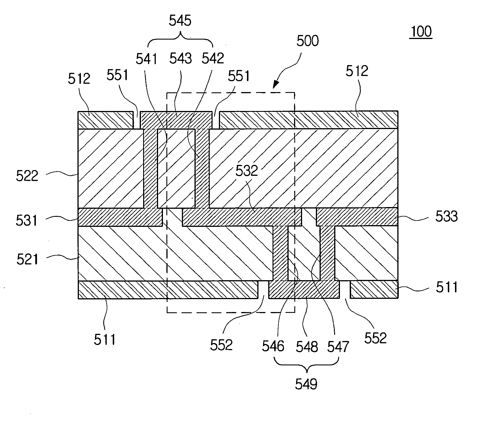
[0140]FIG. 5 is a plan view showing a multi-layered electromagnetic bandgap structure having a stitching via and a printed circuit board having the same in accordance with the present invention. FIG. 10A is a 3-D perspective view showing the electromagnetic bandgap structure of FIG. 5.

[0141]The electromagnetic bandgap structure according to a first embodiment of the present invention can include two metal layers 511 and 512, a plurality of metal plates 531, 532 and 533 placed on a planar surface between the two metal layers 511 and 512, a first stitching via 545 electrically connecting one metal plate 532 to another metal plate 531 and a second stitching via 549 electrically connecting the one metal plate 532 to yet another metal plate 533.

[0142]A dielectric layer 521 and a dielectric layer 522 can be interposed between the metal layer 512 and the plurality of metal plates 531, 532 and 533 and between the plurality of metal plates 531, 532 and 533 and the metal layer 511, respective...

second embodiment

[0155]FIG. 6 is a plan view showing a multi-layered electromagnetic bandgap structure having a stitching via and a printed circuit board having the same in accordance with the present invention. FIG. 11A is a 3-D perspective view showing the electromagnetic bandgap structure of FIG. 6.

[0156]The electromagnetic bandgap structure according to a second embodiment of the present invention can include three metal layers 611 and 612, a plurality of metal plates 631, 632 and 633 placed on a planar surface between any two metal layers 611 and 612, a first stitching via 645 electrically connecting one metal plate 632 to another metal plate 631 and a second stitching via 649 electrically connecting the one metal plate 632 to yet another metal plate 633.

[0157]The electromagnetic bandgap structure in accordance with the second embodiment of the present invention can feature the additional metal layer that is placed between at least one of the two metal layers 611 and 612 and the metal plates 63...

third embodiment

[0174]FIG. 7 is a plan view showing a multi-layered electromagnetic bandgap structure having a stitching via and a printed circuit board having the same in accordance with the present invention.

[0175]The electromagnetic bandgap structure in accordance with a third embodiment of the present invention can include a plurality of metal plates 731, 732 and 733 placed on any one planar surface of a printed circuit board, two metal layers 711 and 712 placed on different planar surfaces below the planar surface on which the metal plates 731, 732 and 733 are stacked, a first stitching via 745 electrically connecting any one 732 of the metal plates 731, 732 and 733 to another metal plate 731 and a second stitching via 749 electrically connecting any one metal plate 732 to yet another metal plate 733.

[0176]A dielectric layer 721 and a dielectric layer 722 can be interposed between the metal plates 731, 732 and 733 and any one metal plate 711 and between the two metal layers 711 and 712.

[0177]F...


PUM


Abstract

According to an embodiment of the present invention, an electromagnetic bandgap structure can include: at least three conductive plates; a first stitching via, configured to electrically connect any one of the conductive plates to another conductive plate; and a second stitching via, configured to electrically connect the one conductive plate to yet another conductive plate. In the electromagnetic bandgap structure of the present invetion, the first stitching via can electrically connect the one conductive plate to another conductive plate by allowing a part of the first stitching via to be connected through a planar surface above the one conductive plate, and the second stitching via can electrically connect the one conductive plate to yet another conductive plate by allowing a part of the second stitching via to be connected through a planar surface below the one conductive plate.

Description

CROSS-REFERENCE TO RELATED PATENT APPLICATIONS[0001]This application claims the benefit of Korean Patent Application Nos. 10-2008-0025604 and 10-2008-0062015, filed on Mar. 19, 2008 and Jun. 27, 2008, in the Korean Intellectual Property Office, the disclosure of which is incorporated herein in their entirety by reference.BACKGROUND OF THE INVENTION[0002]1. Field of the Invention[0003]The present invention relates to an electromagnetic bandgap structure, more specifically to an electromagnetic bandgap structure and a printed circuit board having the same that prevent a signal ranging a predetermined frequency band from being transmitted.[0004]2. Background Art[0005]New electronic apparatuses and communication apparatuses are increasingly becoming smaller, thinner and lighter, reflecting today's emphasis on growing mobility.[0006]These electronic and communication apparatuses have various complex electronic circuits (i.e. analog circuits and digital circuits) for performing their func...

Claims


Application Information

Patent Timeline
Patent Type & Authority Applications(United States)
IPC IPC(8): H05K1/02
CPCH01P1/2005H01P1/203H05K1/0236H05K1/0237H05K2201/09309H01L2224/16H05K2201/096H05K2201/09627H05K2201/09663H05K2201/09681H05K2201/09518
Inventor KIM, HANHAN, MI-JAJUNG, HYO-JIC
Owner SAMSUNG ELECTRO MECHANICS CO LTD
Why Eureka
Try Eureka