Bidirectional PNPN silicon-controlled rectifier
- Summary
- Abstract
- Description
- Claims
- Application Information
AI Technical Summary
Benefits of technology
Problems solved by technology
Method used
Image

Examples
second embodiment
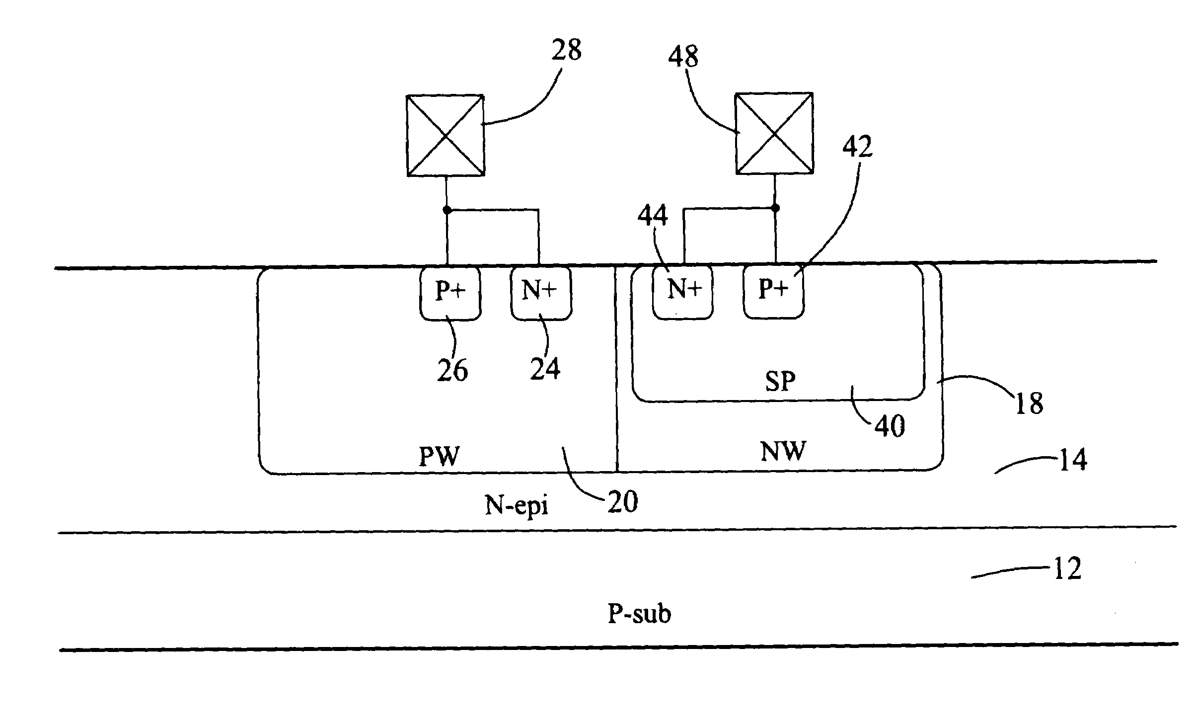
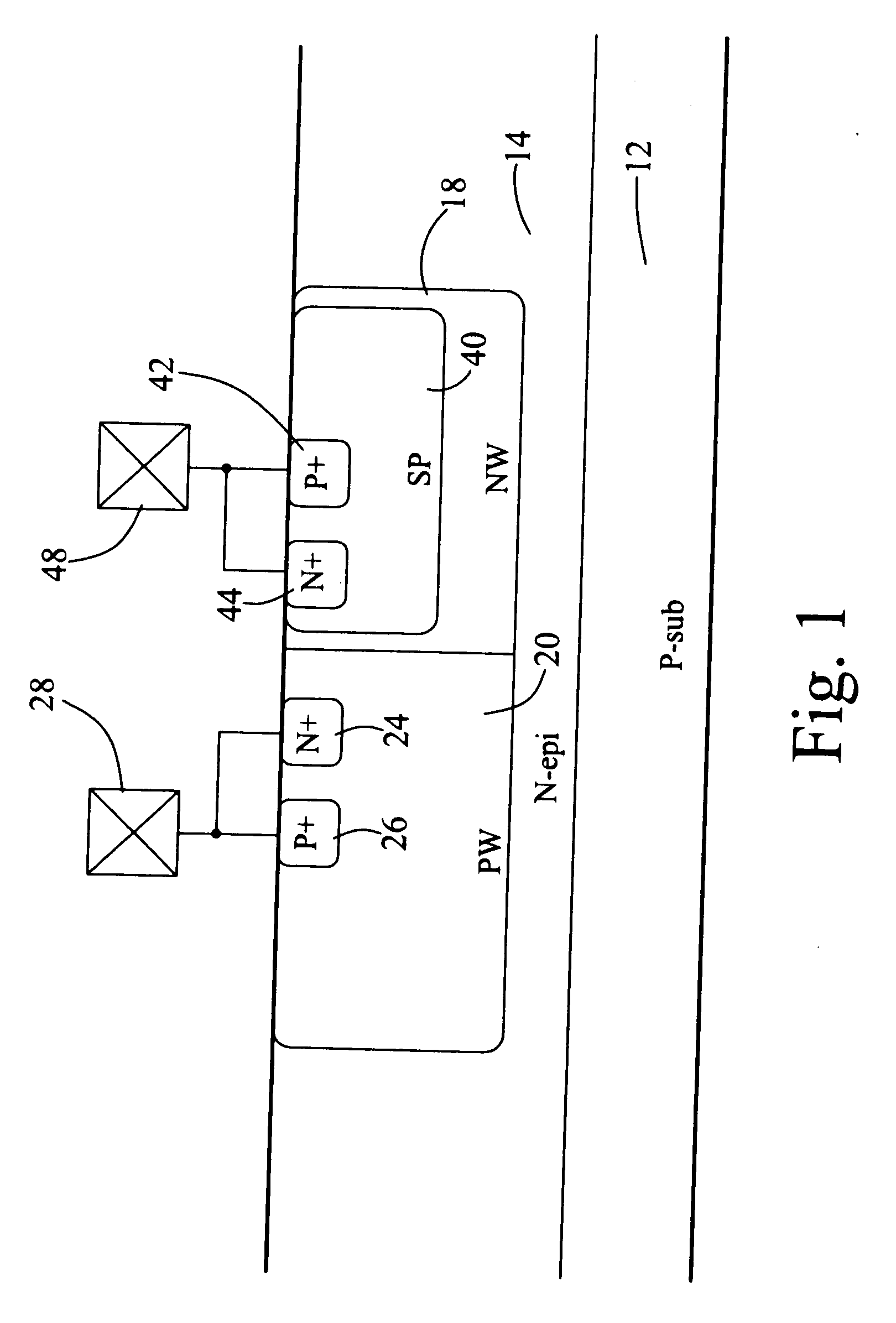
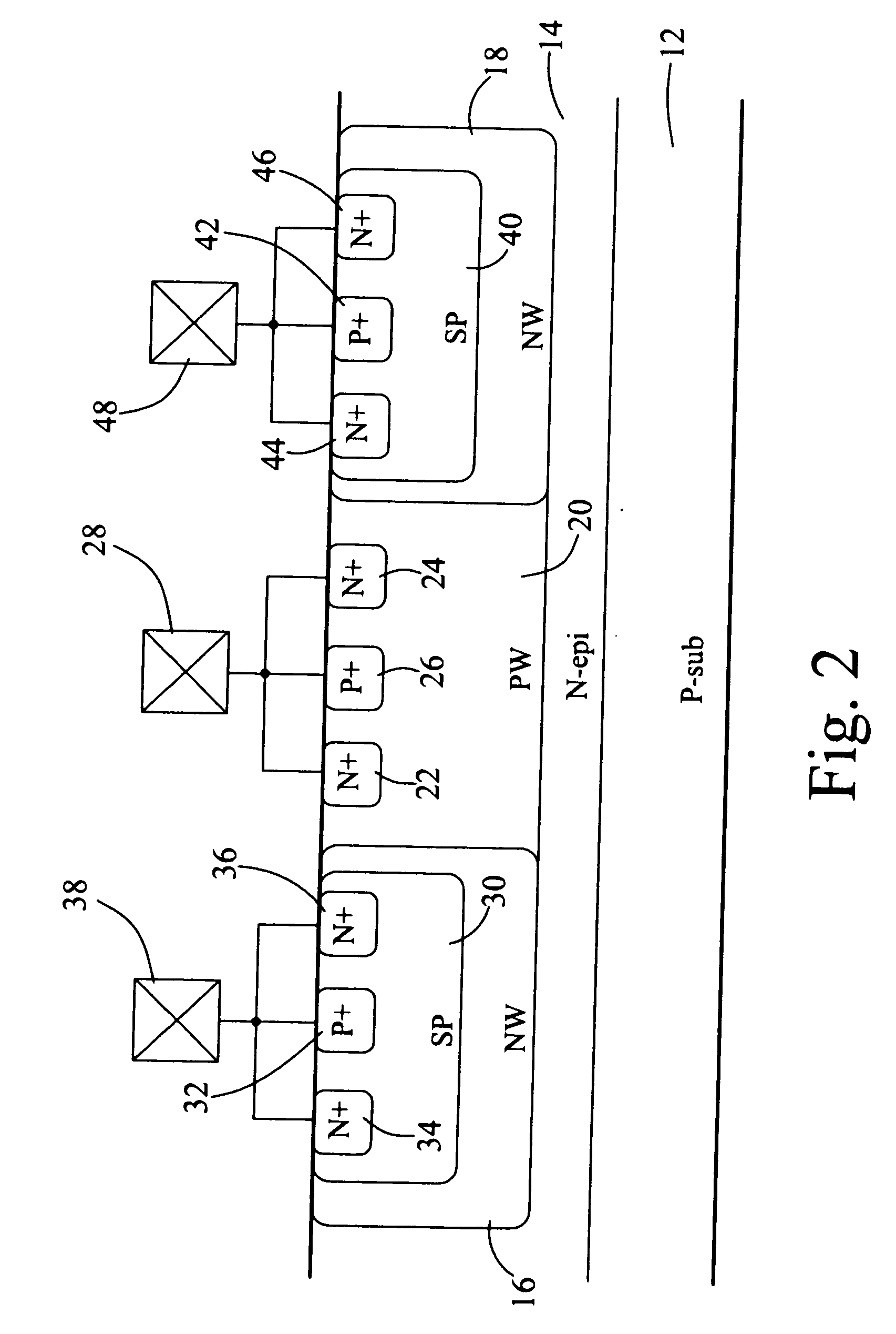
[0036]Refer to FIG. 2 a diagram schematically showing the present invention. The bidirectional PNPN SCR of the present invention comprises a P-type substrate 12. An N-type epitaxial layer 14 is formed on the P-type substrate 12. Two N-type wells 16 and 18 and a P-type well 20 are formed inside the N-type epitaxial layer 14, and the P-type well 20 is interposed between the N-type wells 16 and 18. The P-type well 20 has two N+ semiconductor areas 22 and 24 and a P+ semiconductor area 26 arranged in between the N+ semiconductor areas 22 and 24. The N+ semiconductor areas 22 and 24 and the P+ semiconductor area 26 are all coupled to an anode 28. Thus is formed an anode structure, which includes: the P-type well 20, the N+ semiconductor areas 22 and 24 and the P+ semiconductor area 26.
[0037]The N-type well 16 has a P-type doped area 30 thereinside. The P-type doped area 30 has a P+ semiconductor area 32 and two N+ semiconductor areas 34 and 36 respectively at two sides of the P+ semicond...
eighth embodiment
[0050]Refer to FIG. 8B a diagram schematically showing another aspect of the present invention, wherein the P+ semiconductor area 72 extends through the interface between the middle P-type doped area 67 and the P-type well 66.
[0051]In conclusion, the present invention discloses a bidirectional PNPN SCR whose elements can be fabricated with a deep-submicron semiconductor technology. Thus, the area of SCR can be greatly reduced in the present invention. Further, the bidirectional PNPN SCR of the present invention has a high ESD resistance. Furthermore, the bidirectional PNPN SCR of the present invention has an adjustable trigger voltage and an adjustable hold voltage and can be applied to all process generations. Therefore, the present invention can be effectively integrated into a high voltage device. Besides, the bidirectional PNPN SCR of the present invention has a low parasitic capacitance and a high ESD resistance. Therefore, in the present invention, the influence of SCR parasit...
PUM
 Abstract
Description
Claims
Application Information