Semiconductor integrated circuit package and method of packaging semiconductor integrated circuit

a technology of integrated circuit and semiconductor, which is applied in the field of semiconductor integrated circuit packaging and semiconductor integrated circuit, can solve the problems of poor solderability, circuit board level problems, and lead short circuits, and achieve the effects of reducing the possibility of lead short circuit, increasing the height, and increasing the resistan

Inactive Publication Date: 2009-09-24
NXP USA INC
View PDF5 Cites 48 Cited by
  • Summary
  • Abstract
  • Description
  • Claims
  • Application Information

AI Technical Summary

Benefits of technology

[0028]When the semiconductor IC package according to the present invention is mounted on a printed circuit board (PCB) through a surface mount process, redundant solder paste may easily flow out from a channel formed by the inwardly recessed portion of the mold compound. Even if part of the redundant solder paste does not flow out but extends along mold compound surfaces between the leads, between the die pads, and between the leads and the die pads, since a surface area of a curved surface is much greater than that of a traditional planar surface, the solder paste needs to extend a longer distance from both sides of the clearances between the leads, between the die pads, and between the leads and the die pads thereby to contact each other and cause lead short-circuit, and as a result, the possibility of the lead short-circuit is also reduced.
[0029]Unlike the above-described thicker plating method, the present invention does not increase directly the height (lead stand-off) of the leads (and / or the die pads), but achieves indirectly the effect of increasing the height (lead stand-off) of the leads (and / or the die pads) by lowering the mold compound around the leads (and / or the die pads) and making the mold compound recessed inward. Compared with the thicker plating method, the present invention may obtain a greater lead stand-off.
[0030]Further, the packaging method of the present invention makes little change in process and this stable process control of the molding process can be achieved.

Problems solved by technology

If the lead area is covered with mold compound, or not fully exposed or not easily contactable, a solderability problem of the leads and a printed circuit board (PCB), for example, may arise.
In the IC package application, it has been found that, due to a lower lead stand-off or even the lack of the lead stand-off in a Quad Flat No-lead (QFN) or Power Quad Flat No-lead (PQFN) package, some circuit board level problems tend to occur, for example, the solderability is poor, and particularly, a lead short-circuit or the like is liable to occur.
Some methods, such as a thicker plating method and an epoxy bumping method, have been taken into consideration for solving the above problem, but these methods bring about some other problems.
However, this method has the following problems: a long plating time results in a very low UPH (Units Per Hour) in the plating process; the thicker plating process is difficult to control; in adicing / cutting process, it is hard to perform alignment using calibration points set on the back surface of the lead frame due to the existence of the thicker plating layer; also, there exists a higher risk of whisker growing.
Further, the stand-off obtained by means of the thicker plating method does not have a great height.
In the so-called epoxy bumping method, epoxy bumps are set on the back surface of the lead frame using an adhesive injection method to leave space between the lead frame and the printed circuit board, thereby causing redundant solder paste to flow out during the surface mounting process.
However, in this method, besides the difficulty of controlling the co-planarity of bumps, additional equipment costs for setting epoxy bumps are increased.

Method used


Image

  • Semiconductor integrated circuit package and method of packaging semiconductor integrated circuit
  • Semiconductor integrated circuit package and method of packaging semiconductor integrated circuit
  • Semiconductor integrated circuit package and method of packaging semiconductor integrated circuit

Examples


Embodiment Construction

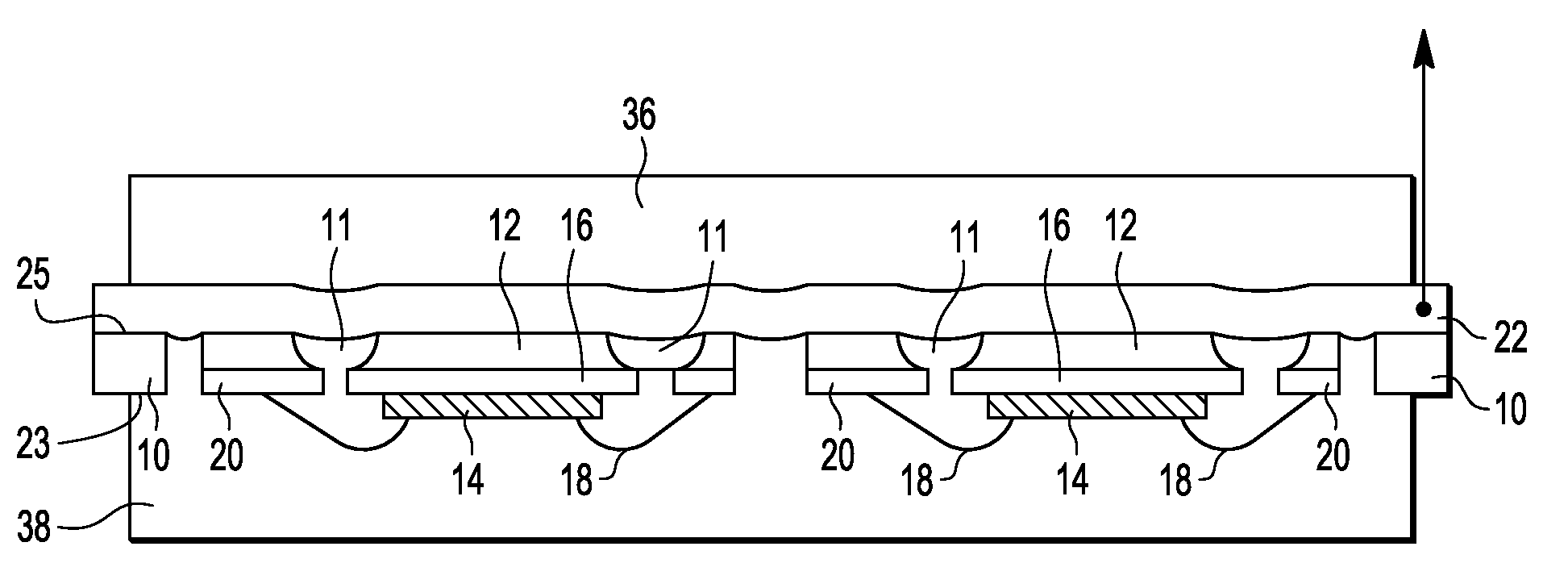
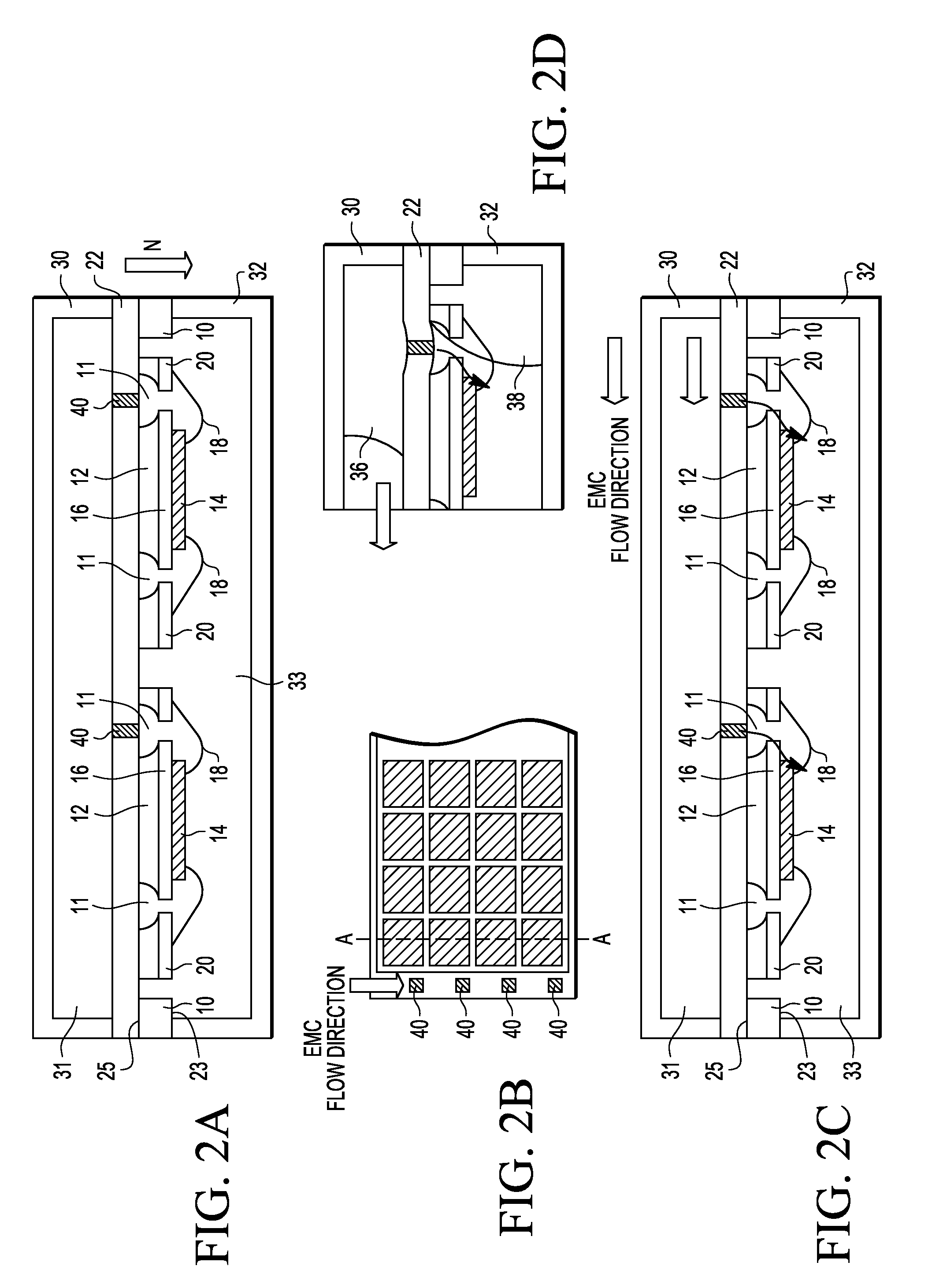
[0035]The present invention will now be described in detail with reference to the drawings. FIG. 2A shows a dual-cavity mold according to the present invention and a lead frame array held therein. The dual-cavity mold has an upper mold chase 30 and a lower mold chase 32 that form two cavities.

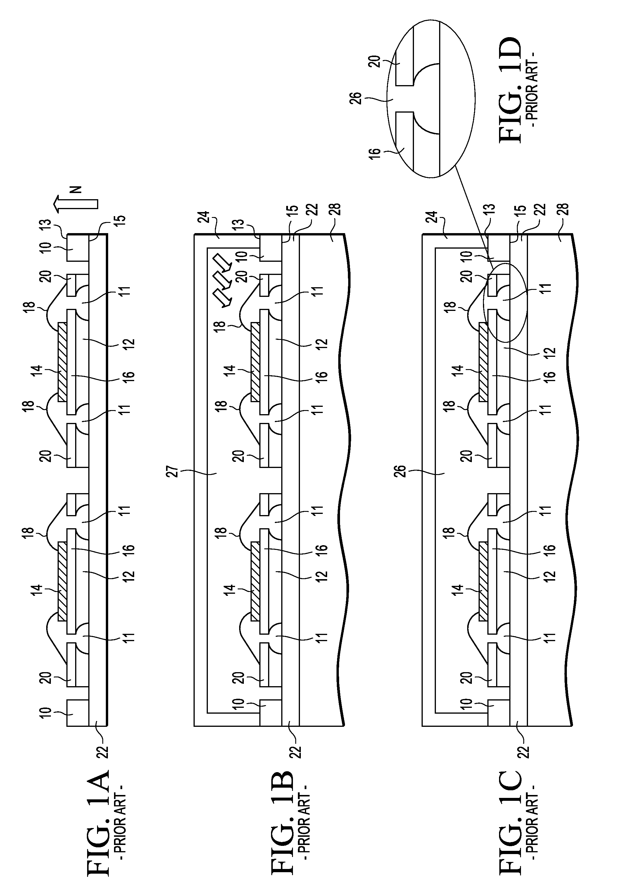
[0036]The lead frame array used here is the same as the foregoing lead frame array described with reference to FIG. 1A. The beforehand prepared lead frame array includes one or more lead frames 10. Each lead frame 10 has leads 20 and die pads 16. After the leads 20 and the die pads 16 on the lead frame are formed by full-etch, edge portions of the leads 20 and / or the die pads 16 are usually further half-etched from a back surface 25 of the lead frame 10 to form half-etched portions 12, thereby causing clearances 11 between the leads 20 and / or the die pads 16 to have an increased size on the back surface 25.

[0037]FIGS. 2A-2D and FIGS. 3A and 3B only show the clearances 11 between the leads 20 an...


PUM

PropertyMeasurementUnit
recessed depthaaaaaaaaaa

Abstract

In a method of packaging a semiconductor IC, a tape is attached to a back surface of a lead frame array, and the lead frame array is held between an upper mold chase and a lower mold chase of a mold, with the back surface of the lead frame array upward. The upper and lower mold chases form an upper cavity and a lower cavity with respect to the lead frame array respectively. A mold compound is injected into the upper and lower cavities respectively. With respect to clearances between leads, between die pads and/or between the leads and the die pads, the mold compound injected into the upper cavity covers the portion of the tape over the clearances before the mold compound injected into the lower cavity fills the clearances, so that the tape is depressed. After curing the mold compound, removing the mold and de-taping, the mold compound filled in the clearances is recessed inward from the back surface, which increases the solderability in the subsequent surface mount process and decreases the possibility of the occurrence of lead short-circuits.

Description

FIELD OF THE INVENTION[0001]The present invention relates in general to semiconductor integrated circuits (ICs), and more particularly to a semiconductor integrated circuit package and a method of packaging a semiconductor integrated circuit.BACKGROUND OF THE INVENTION[0002]At present, a lead frame is often used to provide a semiconductor chip with electrical interconnection. That is, the chip is attached to die pad of the lead frame, and then the pads on the semiconductor chip are electrically connected to leads of the lead frame using wires by way of a wire bonding technique. Thereafter, an integrated circuit comprising a semiconductor chip, a lead frame and wires is packaged using mold compound. Exposed areas of the leads are used for providing electrical interconnection from the outside to the semiconductor chip.[0003]In order to provide good electrical interconnection with other devices, a portion of the leads must be fully exposed. If the lead area is covered with mold compoun...

Claims


Application Information

Patent Timeline
Patent Type & Authority Applications(United States)
IPC IPC(8): H01L23/495H01L21/60H01L21/56B29C45/14
CPCH01L21/561H01L21/566H01L21/568H01L23/3107H01L2224/32245H01L2224/48247H01L2224/73265H01L2224/48091H01L2924/00012H01L2924/00014H01L24/73H01L2924/14H01L2924/00
Inventor XU, XUESONGXU, NANYAO, JINZHONG
Owner NXP USA INC
Why Eureka
Try Eureka