Device interconnects

a technology of device interconnection and interconnection layer, which is applied in the direction of printed circuit non-printed electric components association, semiconductor/solid-state device details, chemistry apparatus and processes, etc., can solve the problems of low interlayer via density, high cost, and inability to find suitable techniques, etc., to achieve the effect of reducing capacitance and resistance of interlayer interconnects, high inter-layer interconnect density, and improving circuit speed

Active Publication Date: 2009-10-01
SHARP KK
View PDF17 Cites 13 Cited by
  • Summary
  • Abstract
  • Description
  • Claims
  • Application Information

AI Technical Summary

Benefits of technology

[0047]Positioning the second set of devices such that a via containing an electrical interconnect lies at least partially within the footprint of the devices which are connected by the electrical interconnect reduces the area of the substrate not occupied by devices, thereby allowing more devices to be provided per unit area of substrate. Most importantly, it allows to achieve the most direct (meaning shortest) interlayer interconnects resulting in a reduction of the resistance and capacitance of these interconnects.
[0117]1. The disadvantages particular to face-to-face bonding and face-to-back bonding are removed as the distinction between the two vanishes if devices on which contacts can be formed on either side (the one facing away from the substrate and the one facing the substrate) are used. (Most conventional planar devices do not exhibit this property). This means in particular that more than two device layers can be assembled in the invention while the most direct and therefore simple inter-layer device interconnects can be realized (no “routing” of interlayer-interconnects around devices is required). This means that a high inter-layer interconnect density can be achieved without compromising on device density. Furthermore, the capacitance and resistance of the interlayer interconnects is reduced which results in advantages regarding power dissipation and circuit speed.

Problems solved by technology

However, at present no suitable techniques are available for applying a high density of devices to a receiver substrate such that all of the following desiderata are met:1. More than two device layers can be integrated onto a receiver substrate.2. The achievable number of inter-layer interconnects can be greater than the lowest number of devices contained in a device layer.3. The inter-layer device interconnects do not increase the footprint of the corresponding circuits considerably.4. The way the inter-layer device interconnects are formed and the way the devices are arranged within each layer does not impose constraints onto the type of circuit architecture to be realized (e.g. no limitation to cross-bar architectures) allowing to combine different architectures.5. The vias of the inter-layer device interconnects can be defined using conventional lithography.6. No thinning of the transferred structures before or after the transfer is required.7. No Silicon-on-Insulator (SOI) material is required.
Face-to-face bonding is limited to a maximum of two device layers, while face-to-back bonding suffers from a low interlayer via density.
This problem can be mitigated by using a SOI-based face-to-back bonding process, but this is more costly.
Furthermore, the nanowires show poor edge alignment, imposing a challenge on forming interconnects between particular sections of nanowires belonging to different device layers.

Method used


Image

  • Device interconnects
  • Device interconnects
  • Device interconnects

Examples


Embodiment Construction

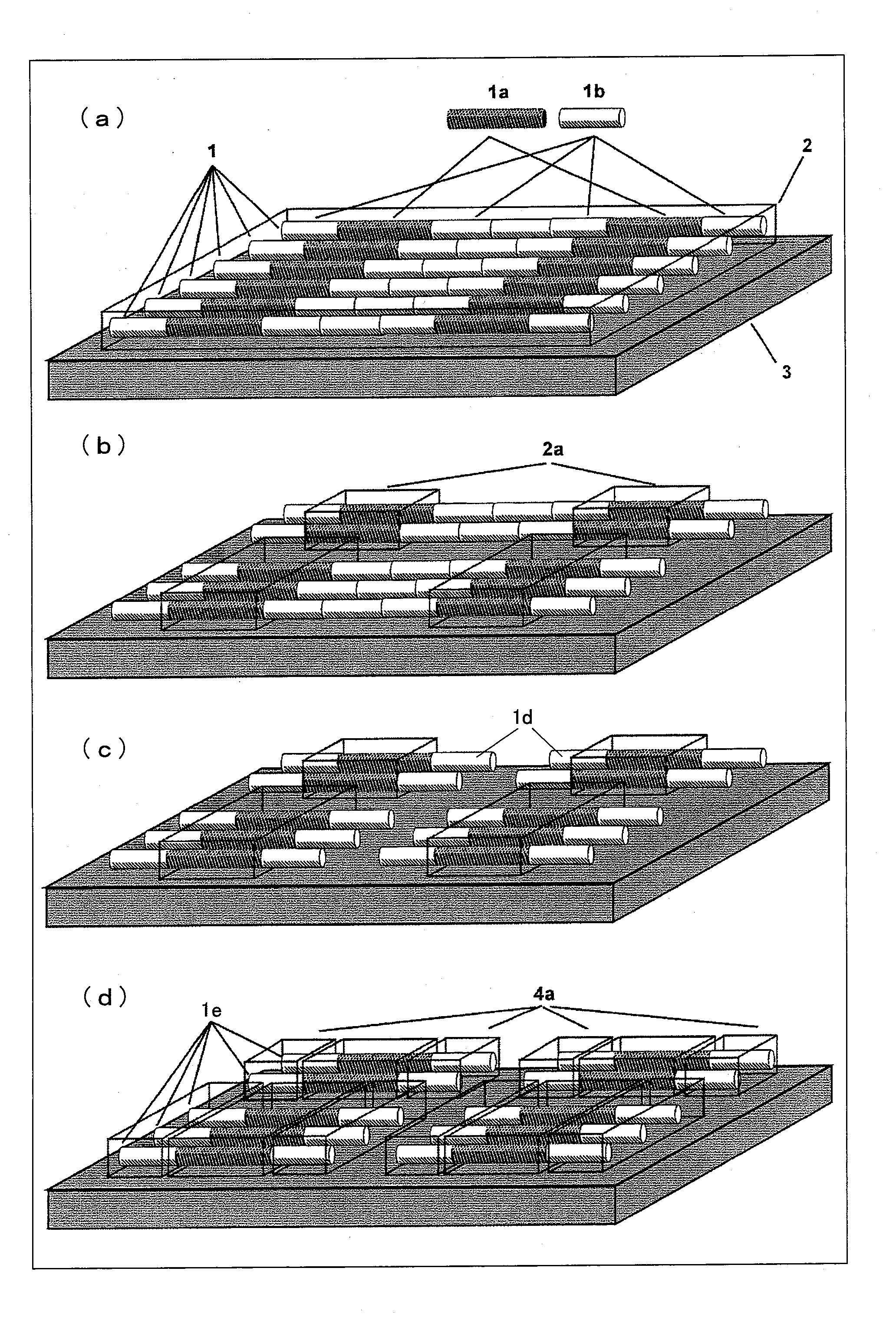
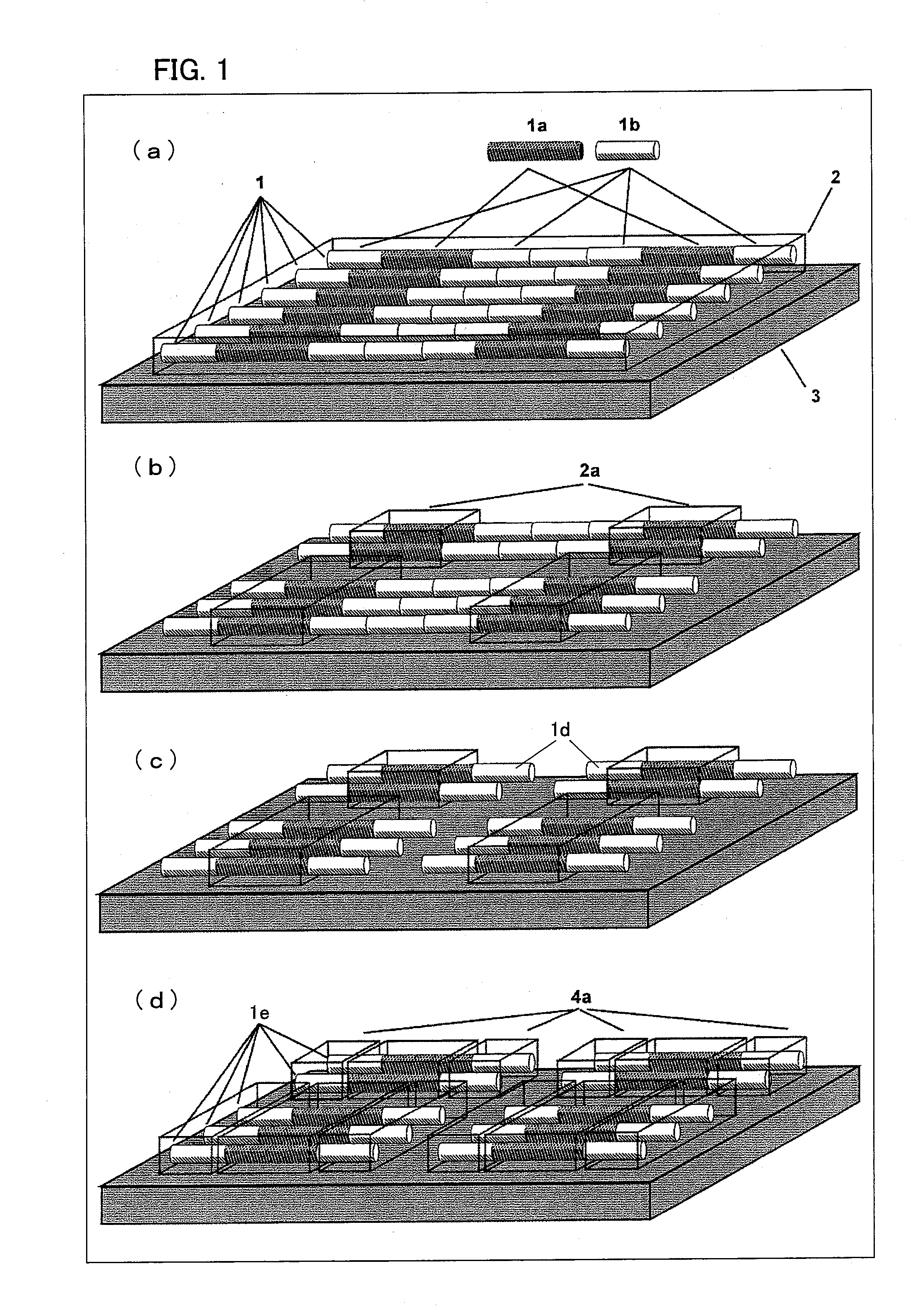
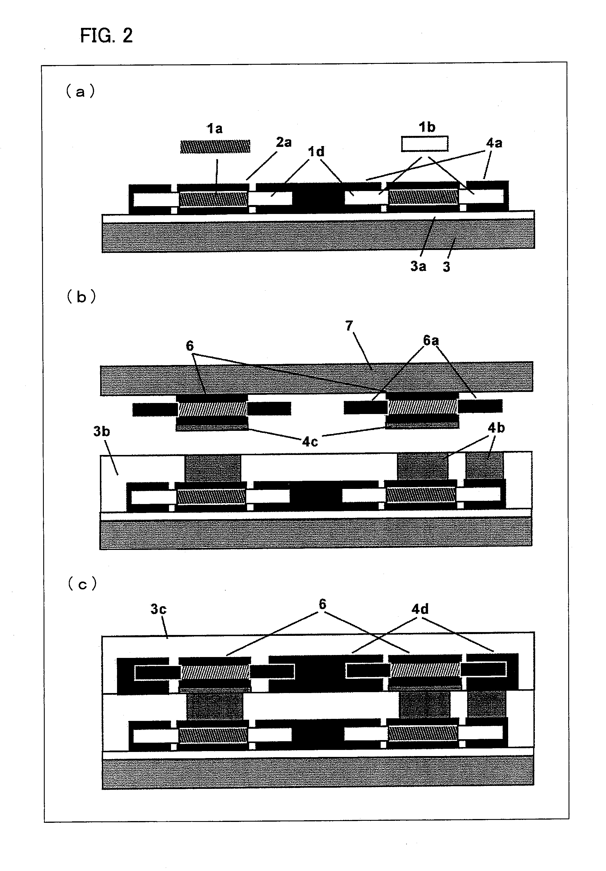
[0128]FIGS. 1(a) to 1(d) show the initial steps of a fabrication method in which a plurality of devices is fabricated on a substrate. In this particular example, the starting material consists of a plurality of parallel and edge aligned elongate low-dimensional structures 1 which are encapsulated in a matrix 2 and positioned on a substrate 3 so as to extend substantially parallel to the substrate, as shown in FIG. 1(a). In the example of FIG. 1(a) the elongate low-dimensional structures 1 do not have a uniform constitution along their length but contain regions 1a, 1b of different constitution from one another. For example, one or more of the following may differ between the regions 1a and the regions 1b: material composition, material composition profile, cross-section geometry, cross-sectional dimensions and orientation.

[0129]The substrate 3 may be formed of any suitable material and may, for example, be a transparent substrate, for example a glass substrate or a transparent plast...


PUM

PropertyMeasurementUnit
insulatingaaaaaaaaaa
low-dimensional structuresaaaaaaaaaa
symmetryaaaaaaaaaa

Abstract

A method of fabricating a device structure, comprises: forming an insulating layer (3b) over a first set of devices disposed over a substrate (3); forming one or more vias in the insulating layer; disposing a second set of devices (6) over the insulating layer, wherein devices of the second set comprise respective electrical contacts (6a) and are disposed over the insulating layer (3b) such that a side on which a contact (6a) can be accessed faces the substrate (3); and forming one or more electrical contacts between the first set of devices and the second set of devices (6) through the via(s). The second set of devices and at least one via are positioned such that one or more of the vias lies at least partially within the footprint of two devices, each belonging to a different device layer.

Description

[0001]This nonprovisional application claims priority under U.S.C. §119(a) on Patent Application No. 0805848.9 filed in United Kingdom on 1 Apr., 2008, the entire contents of which are hereby incorporated by reference.FIELD OF THE INVENTION[0002]This invention relates to the integration of multiple device layers onto receiver substrates. Monolithic integration of several device layers on a substrate is in most cases technically not viable because the required material can't be deposited with sufficient quality onto the substrate (e.g. due to structural incompatibilities) and / or the process flow to form a later layer may be incompatible with devices previously fabricated on the substrate (e.g. high temperature steps are undesirable after metallization of previous devices, or contamination issues).BACKGROUND OF THE INVENTION[0003]Display technologies are an example where the structural incompatibilities in conjunction with the low thermal budget of most transparent substrates (typical...

Claims


Application Information

Patent Timeline
Patent Type & Authority Applications(United States)
IPC IPC(8): H05K1/11B32B37/00
CPCH01L21/6835H01L2924/01075H01L24/66H01L24/69H01L25/0652H01L25/50H01L2221/68368H01L2225/06527H01L2225/06579H01L2924/01013H01L2924/01029H01L2924/01033H01L2924/01057H01L2924/01079H01L2924/01082H01L2924/12044H01L2924/14H01L2924/19041H01L2924/19043H01L2924/30105H05K1/185H05K3/303H01L2924/01005H01L2924/01006H01L2924/01023H01L2924/01074H01L23/5387H01L2924/15788H01L2924/12042H01L2924/00H01L23/5386H01L25/0657H05K1/11
Inventor ALTEBAEUMER, THOMAS HEINZ-HELMUTDAY, STEPHENLANG, CHRISTIANHEFFERNAN, JONATHAN
Owner SHARP KK
Why Eureka
Try Eureka