Organic light-emitting display device

a technology of light-emitting display device and organic light-emitting element, which is applied in the direction of solid-state device, semiconductor device, thermoelectric device, etc., can solve the problem of prolonging the life of the devi

Inactive Publication Date: 2009-10-01
PANASONIC LIQUID CRYSTAL DISPLAY CO LTD +1
View PDF10 Cites 50 Cited by
  • Summary
  • Abstract
  • Description
  • Claims
  • Application Information

AI Technical Summary

Benefits of technology

[0020]According to the present invention, the life of organic light-emitting elements which emit light of a color having a short life can be prolonged in an organic light-emitting display device using a number of organic light-emitting elements which emit light of different colors.

Problems solved by technology

Therefore, the amount of current required to gain a certain brightness becomes small, and therefore, the life is prolonged.

Method used


Image

  • Organic light-emitting display device
  • Organic light-emitting display device
  • Organic light-emitting display device

Examples


first embodiment

[0106]The organic light-emitting display apparatuses according to embodiments of the present invention are described in reference to the drawings.

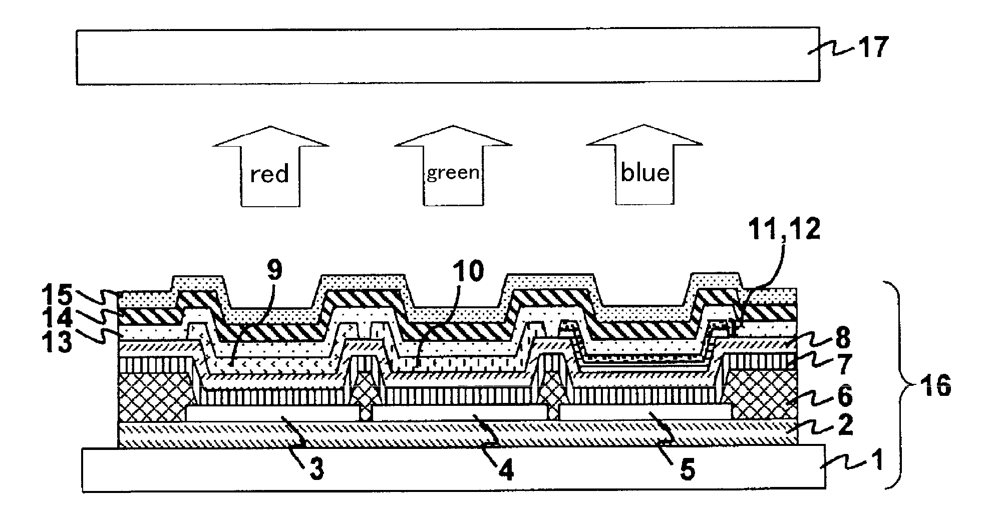
[0107]FIG. 1 is a cross sectional diagram showing a pixel in an organic light-emitting display device. In addition, FIG. 2 is a schematic cross sectional diagram showing a blue light-emitting element.

[0108]Though not shown in FIG. 1, a number of scan lines are aligned with constant intervals between the glass substrate 1 and the first layer insulating film 2, and at the same time, signal lines for transmitting image information are aligned with constant intervals in such a direction as to cross the scan lines.

[0109]That is to say, scan lines and signal lines are aligned in a grid, and the regions surrounded by scan lines and signal lines are display regions for pixels or sub-pixels.

[0110]Furthermore, a number of first current supply lines connected to the power supply are aligned on the glass substrate 1 so as to be parallel to the signal ...

second embodiment

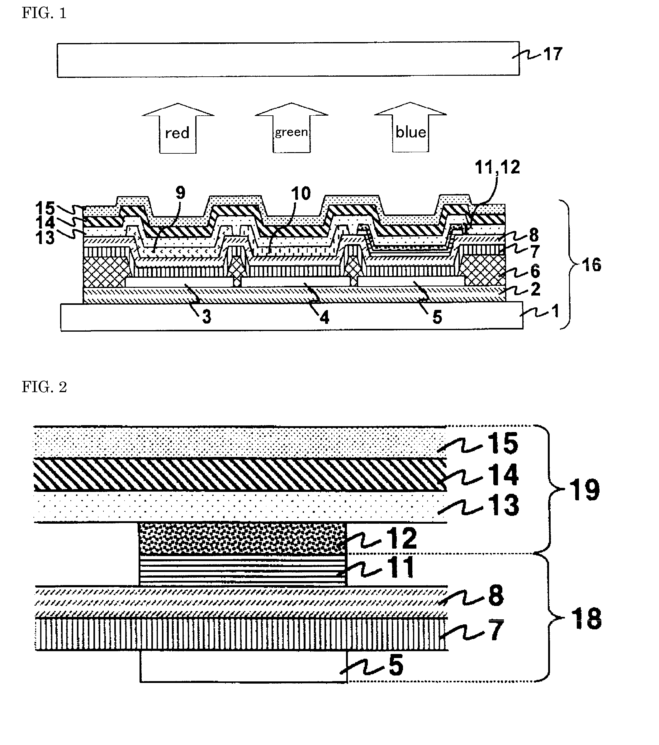
[0142]An example of an organic light-emitting display device according to the second embodiment where the life of blue light-emitting elements can be prolonged, and the efficiency can be increased, by adding a blue light-emitting dopant to the electron transportation layer is described below.

[0143]The method for forming a first interlayer insulating film 2, lower electrodes 3 to 5, a second interlayer insulating film 6, a hole injection layer 7 and a hole transportation layer 8 on a glass substrate 1 is the same as in the first embodiment. In addition, the methods for forming a red light-emitting layer 9 in R sub-pixels, a green light-emitting layer 10 in G sub-pixels, an n doped electron transportation layer 11 and a p doped hole transportation layer 12 in B sub-pixels are also the same as in the first embodiment.

[0144]ADN and 2,5,8,11-tetra-t-butylperylene (hereinafter referred to as “TBP”) are vapor deposited together on top of a charge generating layer made up of a red light-emi...

third embodiment

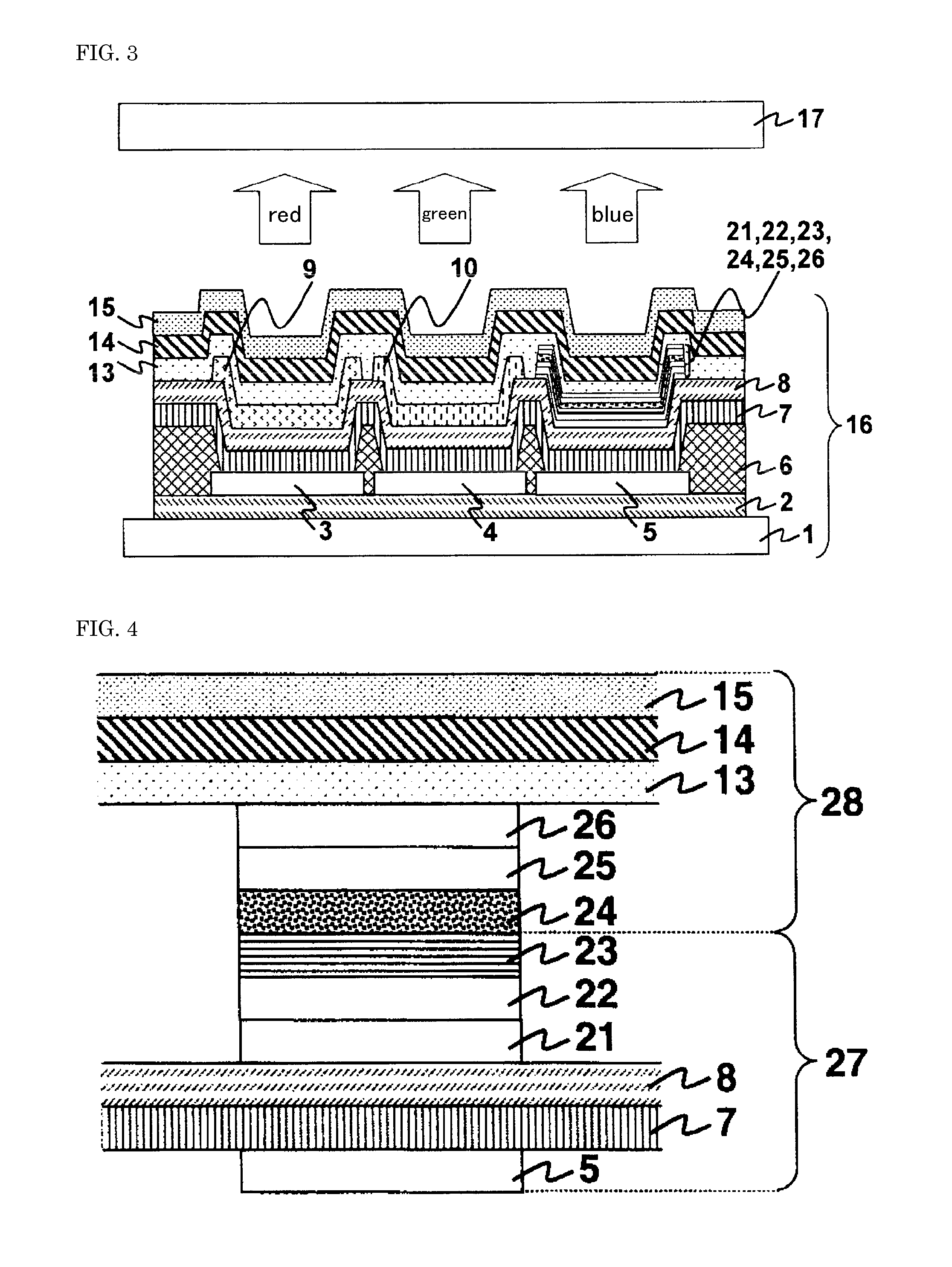
[0150]An example of an organic light-emitting display device according to the third embodiment where the life of blue light-emitting elements can be prolonged, and the efficiency can be increased, by adding a blue light-emitting dopant to the hole transportation layer and the electron transportation layer is described below. The methods for forming a first interlayer insulting film 2, lower electrodes 3 to 5, a second interlayer insulating film 6 and a hole injection layer 7 on a glass substrate 1 are the same as in the first embodiment.

[0151]Next, a vapor deposited film 8 is formed on the hole injection layer 7 of α-NPD and TPB. TPB, which functions as a blue dopant, is added to the vapor deposited film 8 made of α-NPD and TPB, and thus, the efficiency in light emission is high.

[0152]A red light-emitting layer 9 is formed in the R sub-pixel region, a green light-emitting layer 10 is formed in the G sub-pixel region, and an n doped electron transportation layer 11 and a p doped hole...


PUM


Abstract

An object of the present invention is to provide an organic light-emitting display device using a number of organic light-emitting elements that emit lights of different colors, wherein the life of the organic light-emitting elements that emits light of a color having a short life can be prolonged. According to the present invention, a hole injection layer 7, an α-NPD vapor deposited film 8, an n doped electron transportation layer 11 and a p doped hole transportation layer 12, which are patterned to the same size as B sub-pixels, a DNA vapor deposited film 13, an electron injection layer 14 and an upper electrode 15 are formed on a lower electrode 5 in a B sub-pixel. The α-NPD vapor deposited film 8 and the DNA vapor deposited film 13 function as a blue light-emitting layer and exhibit the same properties as when a blue light-emitting element made up of a lower electrode 5, a hole injection layer 7, an α-NPD vapor deposited film 8 and an n doped electron transportation layer 11 and a blue light-emitting element made up of a p doped hole transportation layer 12, a DNA vapor deposited film 13, an electron injection layer 14 and an upper electrode 15 are connected in series. Therefore, it becomes possible to lower the value of a current required for certain brightness, and thus, the life can be prolonged.

Description

[0001]The present application claims priority over Japanese Application JP2008-090957 filed on Mar. 31, 2008, the contents of which are hereby incorporated into this application by reference.BACKGROUND OF THE INVENTION[0002](1) Field of the Invention[0003]The present invention relates to an organic light-emitting display device and an organic light-emitting element that forms an organic light-emitting display device.[0004](2) Related Art Statement[0005]Self-luminous organic electroluminescence elements (hereinafter referred to as “organic light-emitting elements”) are expected to be used for thin display devices and lighting apparatuses for liquid crystal display devices.[0006]Organic light-emitting display devices are formed of a number of organic light-emitting elements that form pixels on a substrate and a drive layer for driving these organic light-emitting elements.[0007]The organic light-emitting elements have a structure where a number of organic layers are sandwiched between...

Claims


Application Information

Patent Timeline
Patent Type & Authority Applications(United States)
IPC IPC(8): H01L51/50
CPCH01L27/3211H01L51/5278H01L51/5052H10K59/35H10K50/155H10K50/165H10K50/19
Inventor ISHIHARA, SHINGOSHIMIZU, MASAO
Owner PANASONIC LIQUID CRYSTAL DISPLAY CO LTD
Why Eureka
Try Eureka