Semiconductor device and method for manufacturing a semiconductor device

a semiconductor and semiconductor technology, applied in the direction of semiconductor devices, basic electric elements, electrical appliances, etc., can solve the problems of large leak current through the thin gate insulating film, the disadvantage of slow erasing operation of floating trap type semiconductor memory devices, and the difficulty of electric charge storag

Inactive Publication Date: 2009-10-01
KIOXIA CORP
View PDF8 Cites 14 Cited by
  • Summary
  • Abstract
  • Description
  • Claims
  • Application Information

AI Technical Summary

Benefits of technology

[0035]FIG. 16 is also a cross sectional view showing one step in the manufacturing method of the field-effect transistor shown in FIG. 14.
[0036]FIG. 17 is also a cross sectional view showing one step in the manufacturing method of the field-effect transistor shown in FIG. 14.
[0037]FIG. 18 is also a cross sectional view showing one step in the manufacturing method of the field-effect transistor shown in FIG. 14.
[0038]FIG. 19 is also a cross sectional view showing one step in the manufacturing method of the field-effect transistor shown in FIG. 14.
[0039]FIG. 20 is also a cross sectional view showing one step in the manufacturing method of the field-effect transistor shown in FIG. 14.
[0040]FIG. 21 is also a cross sectional view showing one step in the manufacturing method of the field-effect transistor shown in FIG. 14.

Problems solved by technology

However, the thinning of the top insulating film causes the increase of leak current from the floating gate and makes the storage of electric charge difficult.
Moreover, the floating trap type semiconductor memory device has the disadvantage of slow erasing operation.
In addition, in a semiconductor device such as a CMOS transistor, the gate insulating film is thinned as the semiconductor device is miniaturized, so that the large leak current via the thin gate insulating film becomes main problem.
However, the gate insulating film may react with the side walls in dependence on the condition of the thermal treatment so as to deteriorate the characteristics of the CMOS transistor.
In addition, in the semiconductor device such as the CMOS transistor, if the gate insulating film is made of the insulating film with high dielectric constant, the gate insulating film may form a SiO2 layer at the surface of the silicon substrate, so that a large amount of interface states are formed to deteriorate the characteristics of the transistor.

Method used


Image

  • Semiconductor device and method for manufacturing a semiconductor device
  • Semiconductor device and method for manufacturing a semiconductor device
  • Semiconductor device and method for manufacturing a semiconductor device

Examples


Embodiment Construction

[0041]Hereinafter, the present invention will be described in detail with reference to the drawings.

(First Semiconductor Device)

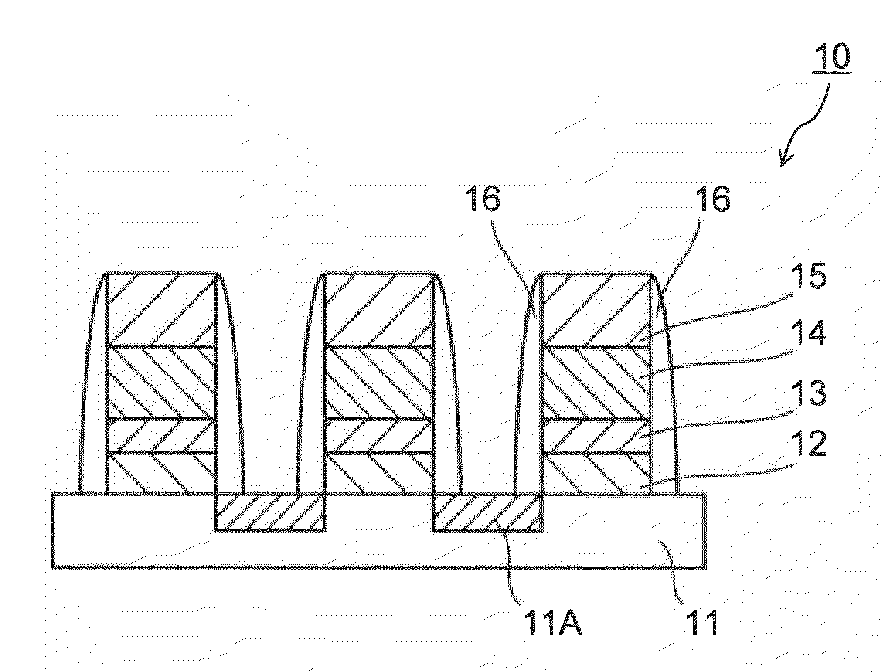
[0042]A first semiconductor device includes a semiconductor substrate, a stacking structure made of a tunnel insulating film, an electric charge storage layer, atop insulating film and a control gate electrode which are subsequently formed on the semiconductor substrate, side walls formed to cover the side surfaces of the stacking structure and impurity doped layers which are formed at the surface of the semiconductor substrate at both sides of the tunnel insulating film.

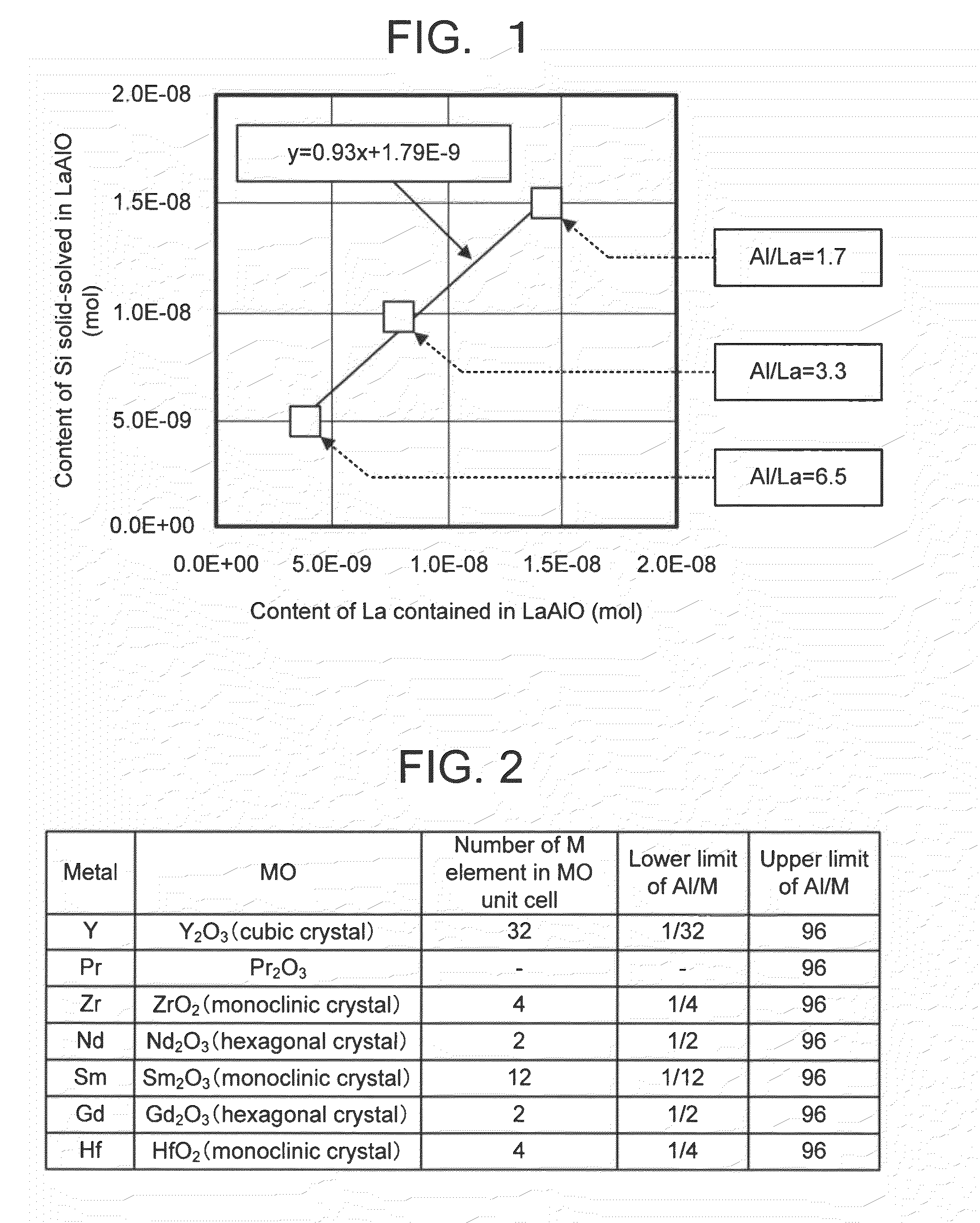
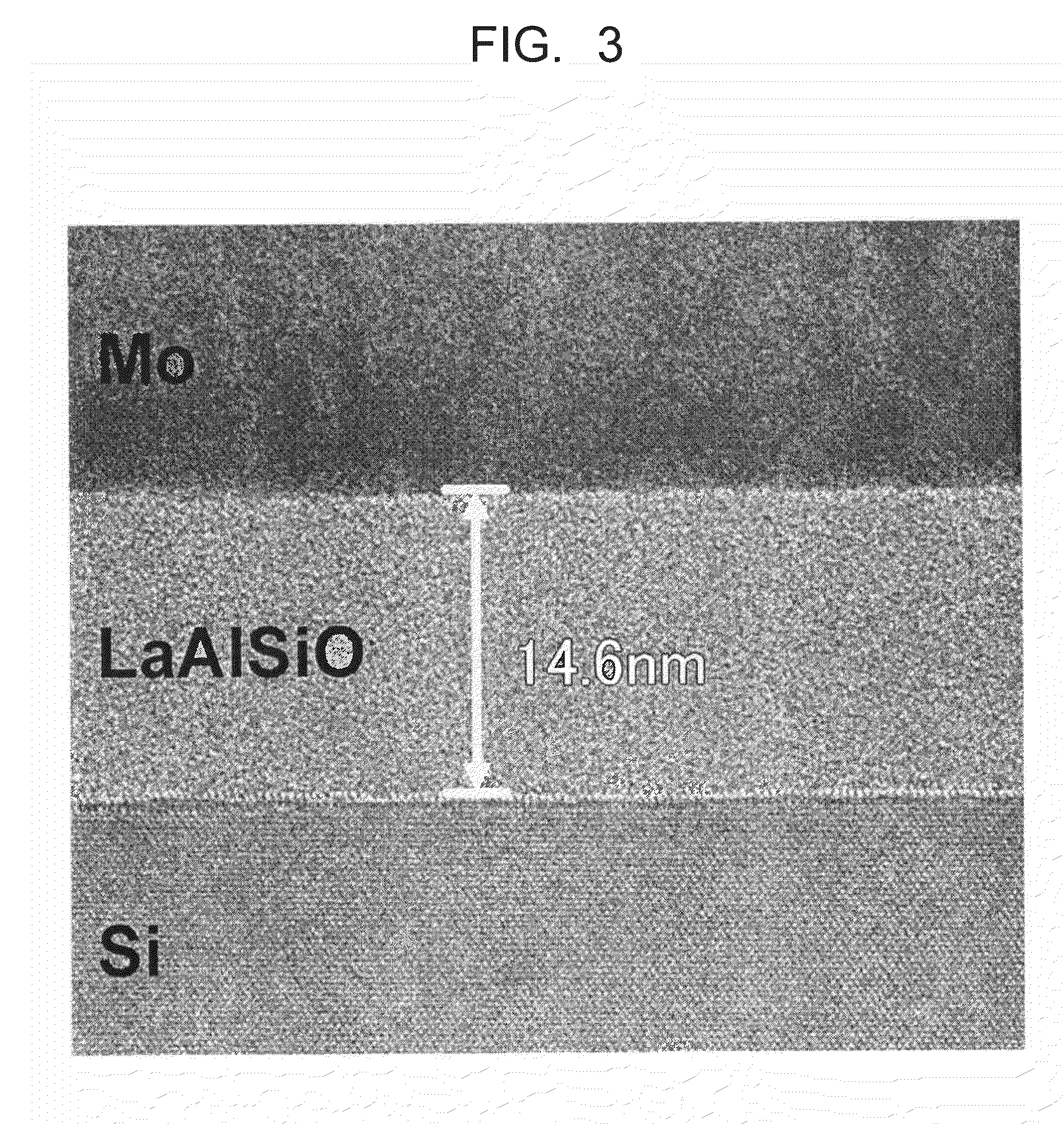
[0043]In the first semiconductor device, it is required that the top insulating film is made of an oxide of at least one metal M selected from the group of rare earth metal, Y, Zr and Hf; Al; and Si (First Requirement). The oxide containing the metal M can exhibit a higher dielectric constant and also a higher crystallization temperature due to containing of the Al element, so that the firs...


PUM

PropertyMeasurementUnit
dielectric constantaaaaaaaaaa

Abstract

In a semiconductor device, the side walls are made of SiO2, SiN or SiON, and the top insulating film or gate insulating film is made of an oxide including Al, Si, and metal element M so that the number ratio Si/M is set to no less than a number ratio Si/M at a solid solubility limit of SiO2 composition in a composite oxide including metal element M and Al and set to no more than a number ratio Si/M at the condition that the dielectric constant is equal to the dielectric constant of Al2O3 and so that the number ratio Al/M is set to no less than a number ratio Al/M where the crystallization of an oxide of said metal element M is suppressed due to the Al element and set to no more than a number ratio Al/M where the crystallization of the Al2O3 is suppressed due to the metal element M.

Description

CROSS-REFERENCE TO RELATED APPLICATIONS[0001]This application is based upon and claims the benefit of priority from the prior Japanese Patent Application No. 2008-086770, filed on Mar. 28, 2008; the entire contents of which are incorporated herein by reference.BACKGROUND OF THE INVENTION[0002]1. Field of the Invention[0003]The present invention relates to a semiconductor device and a method for manufacturing a semiconductor device.[0004]2. Description of the Related Art[0005]A nonvolatile semiconductor memory device typified by an EEPROM is configured such that a tunnel insulating film, an electric charge storage layer, a top insulating film and a control gate electrode are stacked on a semiconductor substrate. Then, a high electric voltage is applied to the control gate electrode so as to infiltrate electrons into the electric charge storage layer from the semiconductor substrate through the tunnel insulating film to conduct writing operation. When the electric charge storage layer...

Claims


Application Information

Patent Timeline
Patent Type & Authority Applications(United States)
IPC IPC(8): H01L29/792H01L29/78H01L21/336
CPCH01L21/28282H01L21/31604H01L29/792H01L29/517H01L29/66833H01L29/513H01L29/40117H01L21/02263
Inventor SHINGU, MASAOKIKUCHI, SHOKOTAKASHIMA, AKIRAINO, TSUNEHIROMURAOKA, KOICHI
Owner KIOXIA CORP
Why Eureka
Try Eureka